- News & Insights
- 2024
- Redefining the Semiconductor Supply Chain: Navigating Challenges, Expanding Opportunities
News & Insights
Redefining the Semiconductor Supply Chain
Navigating Challenges, Expanding Opportunities
Semiconductors are the backbone of modern technology.
They play a crucial role in shaping our lives by powering various innovations, including consumer electronics, internet infrastructure, advanced medical equipment, electric vehicles, and renewable energy systems. Semiconductor equipment is instrumental in the semiconductor manufacturing process, guaranteeing the quality, effectiveness, and dependability of the end products. The industry has grown at a breathtaking pace in recent years despite some challenges along the way. Weakened by the COVID-19 pandemic, geopolitical events, and natural disasters, the semiconductor equipment sector must redesign its supply chain. Although the disruptions and fluctuating demand are still impacting the sector today, the long-term perspective forecasts show healthy growth, mostly due to expanding application spaces like IoT and AI.
Ewa Rosinek, Global Semicon Segment Manager at Nefab, shared what the industry should do to prepare for the growth. “Estimates suggest that the semiconductor sector will double in size by 2030, exceeding $1 trillion by the end of the decade. The potential is immense, and to seize the market, companies must act now. The semiconductors leaders should focus on four dimensions that will define tomorrow's supply chain, i.e., sustainability, transparency, agility, and resilience”. Follow along as we investigate how the semiconductors industry can transform challenges into market opportunities.
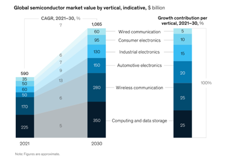
The semiconductor market is experiencing growth primarily propelled by the automotive, data storage, and wireless industries, as indicated by a McKinsey report.
Paving the way toward sustainability in the semiconductor industry
The semiconductor industry has set off to achieve the net zero emissions target by 20503. As transportation accounts for almost a quarter of all CO2-eq emissions globally4, no wonder industry leaders are turning to supply chains to achieve their sustainability goals. Analyzing and optimizing transportation is the first step to lowering the overall costs and the environmental impact of your shipment, and innovative packaging design, although often underrated, is doing just that. Lightweight and sustainable packaging solutions are designed to protect delicate semiconductor products and decrease the overall load weight. A lighter load means fewer shipments and, subsequently, lower CO2-eq emissions.
Thermoformed solutions are a great example of a solution designed for circularity. Thermoformed waste can be collected, cleaned, shredded, and extruded for reuse as raw material for new products. This keeps the plastics in continuous use, which reduces costs and CO2-eq emissions in supply chains. New solutions can be validated through thorough Life Cycle Analysis (LCA) tools, which measure and identify areas of improvement in supply chains by considering factors like Global Warming Potential (GWP), water and energy consumption, types of packaging materials, transport modes, and logistics flows. The software quantifies the existing and proposed solutions' environmental and financial savings to help validate the choice. “We see sustainability not as a challenge but as an opportunity. In our perspective, sustainability serves as a powerful engine for growth”, explained Ewa.
Optimized packaging design and circular solutions save environmental and financial resources in supply chains.
Visibility as a key to agile semiconductor supply chains
The traceability challenges in the semiconductors industry became particularly apparent during the COVID-19 pandemic, prompting the need for a significant shift. Only 6% of companies report complete visibility on their supply chain.5 Alarmingly, 45% of respondents admitted to either lacking visibility into their upstream supply chain or having limited insight, extending only to their first-tier suppliers.6 “Let’s not forget that the supply chain of semiconductors involves extremely sensitive and expensive equipment with a long lead-time, so transparency is an absolute imperative,” stressed Ewa.
Packaging solutions that prioritize transparency help track the movement of semiconductor components, ensuring the security and efficiency of the supply chain. Connected packaging services, for instance, ensure no blind spots in the supply chain. Adding track and trace functionality to the packaging solutions allows monitoring livestock levels and shipments in transit and alerting on various conditions incurred, like shock, tampering, or late deliveries. The data provided also enables analysis of routes, delivery performance, handling, utilization, and lead times.

By using a mix of technologies, Nefab’s track & trace platform provides real-time location in transit. This data can increase efficiencies as well as reduce costs of your connected flows, sometimes even up to 65% cycle time.
Building resiliency through regionalization of the supply chains
The COVID-19 pandemic has challenged the status quo in many industries. It has also exposed the vulnerabilities and complexity of global supply chains. As a result, we currently see a shift from globalization to regionalization of the semiconductor manufacturing industry. Although semiconductors were invented in the United States, their production hub is on the other side of the planet in Southeast Asia. Around the globe, governments are making substantial investments in the semiconductor industry with the aim of achieving shorter lead times and more industry independence. Notably, from 2010 to 2015, China directed significant funds into its semiconductor sector.7 Following suit, the US8 and the EU9 embarked on substantial investments in their semiconductor supply chains.
The semiconductor supply chain will still be global. Yet, growing regionalization creates an opportunity to strengthen supply chain resilience. The companies must embrace their worldwide presence and strengthen their local links to remain relevant. And they should require the same from their suppliers. “Providing a unified level and quality of services to your customers, regardless of the geography, is imperative in today’s market. It’s in Nefab’s DNA. We want to be where our customers are. That’s what sets us apart,” added Ewa.
How is Nefab preparing for tomorrow's supply chain?
“In response to the increasing demand in the semiconductor equipment sector, we have recently opened a new facility with a dust free room in Penang, Malasia. Our plans for 2024 involve expanding our capacities and extending our global offerings. Concurrently, efforts are underway to enhance our capacity in Europe. To help us succeed and propel growth, we rolled out an internal training program for our colleagues across the globe. We know that to succeed tomorrow, we must start adjusting now”, summarized Ewa.
We save resources in supply chains for a better tomorrow.
Want to learn more?
GET IN TOUCH
Contact us to learn more about our smart and sustainable solutions.
LEARN MORE
GreenCalc
Nefab’s own certified calculator measures and quantifies financial and environmental savings in our solutions.
Sustainable Solutions
Engineered packaging for sustainable supply chains.
Sustainable Materials
Fiber-based packaging and raw materials