• Corporate News

The space, weight, and cost-saving NEFAB ExPak has arrived in Silicon Valley!

In addition to the existing ExPak manufacturing sites in Dallas and Canada, Nefab has now opened the third North American ExPak plant in San Jose, California.

Nefab ExPak is a great alternative to traditional cleated crates. It enables companies to improve logistics as it is a volume efficient, strong, and light-weight solution. Due to the foldable design, it can ship flat to save storage space.

“With the addition of the ExPak product line to our current capabilities, we have a great offer with a wide range of engineered packaging solutions to the high tech industry in, and around, the Silicon Valley. The new capabilities have already proven to be a good fit for customers within the Semiconductor Machinery, Energy Storage, Telecom, and Datacom industries.” says Fredrik Solscher, Managing Director Nefab Packaging West, LLC.

Facts about Nefab’s site in San Jose CA:
Address: 8477 Central Avenue, Newark, CA 94560
Certifications: ISO 9001 & ISO 14001
Engineering capabilities: Multi-material packaging design, prototyping, and testing
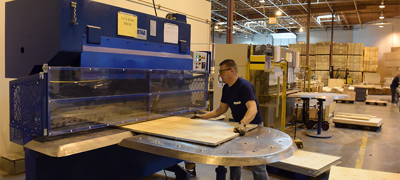
Manufacturing capabilities: Nefab ExPak & ExPak XL, Cleated plywood crates, Corrugated and Foam solutions, PE and Alu barrier bags, Packing supplies, as well as on-site packing services.
Contact us at sales.nca@nefab.com or +1 (408) 678 2500

Our latest news & insights
  • 2025.12.02 Semiconductor

    How to Protect Semiconductor Manufacturing Equipment in Transit?

    Semiconductor manufacturing leaves no room for error. Every process, every component, every piece of equipment operates within microscopic tolerances, and that precision can’t be compromised once the machines leave the cleanroom. Yet, shipping high-value parts such as electrostatic chucks, pedestals, or showerheads introduces a whole new layer of risk.

  • 2025.11.26 Customer Cases

    Sustainable Packaging for Wafer Shipping

    Semiconductor manufacturing is a complex process that can be broadly divided into two main phases: the front-end process and the back-end process. Nefab partnered with a leading semiconductor manufacturer to optimize the packaging solution for shipping wafers between its front-end and back-end facilities, achieving significant financial and environmental benefits.

  • 2025.11.25 Energy

    Why Shipping Grid Equipment Is a Different Kind of Challenge and How to Overcome It?

    Why Shipping Grid Equipment Is a Different Kind of Challenge and How to Overcome It?