Packaging Solutions for Semiconductor Equipment
Custom packaging and logistics solutions designed to protect and transport contamination-sensitive, high-value semiconductor equipment, precision sub-assemblies, and wafers.

Custom packaging and logistics solutions designed to protect and transport contamination-sensitive, high-value semiconductor equipment, precision sub-assemblies, and wafers.
Protect high-value semiconductor equipment that requires stable transport, clean handling, and protection from shock and vibration.

Support safe handling and transport of sensitive semiconductor components, tools, and wafers that require contamination control and physical protection.

Support contamination-controlled handling and transport for sensitive products used in cleanroom environments.
Transporting semiconductor products is not just about moving goods from one location to another. It requires packaging solutions that support clean handling, reliable protection, and consistent performance across complex global supply chains.
Nefab develops custom packaging solutions for semiconductor applications using engineered materials and tailored designs to help protect sensitive products throughout transport, storage, and handling. Our approach focuses on balancing product protection, operational efficiency, and sustainability.
With a global network of 250+ engineers and 6 ISTA-certified test labs worldwide, Nefab develops and validates packaging solutions for sensitive semiconductor applications across global supply chains.
We design, manufacture, and clean packaging solutions to support cleanroom requirements and ensure effective contamination control during transport and handling.
Using our GreenCalc™ LCA tool, Nefab helps identify opportunities to reduce packaging cost and environmental impact through data-driven analysis.

Nefab collaborated with a semiconductor manufacturer to optimize their wafer packaging solution, delivering substantial financial and environmental benefits.
Nefab partnered with a leading semiconductor manufacturer to optimize the packaging solution for shipping wafers between its front-end and back-end facilities, achieving significant financial and environmental benefits.

Our customer was using a legacy packaging design for the RPS (Remote Plasma Source) Adapters that was inefficient and costly. By re-engineering the packaging, we developed a streamlined, resource-efficient solution that reduced material use and volumetric weight.
A leading innovator in the semiconductor industry required a specialized packaging solution for hoisting tools used in their cleanrooms. Through a multi-layered, material-specific design they improved cleanliness, efficiency, and product security.

A customer in the semicon sector faced high air freight costs, product safety concerns, and inefficient handling processes. By implementing the ExPak XL system, the customer achieved a 40% reduction in packaging weight, significantly lowering transportation costs and CO2 emissions.
Semiconductor packaging requirements vary by product sensitivity, cleanliness requirements, handling conditions, and logistics flow. Explore solutions for capital equipment, precision sub-assemblies, and recurring wafer or component logistics.

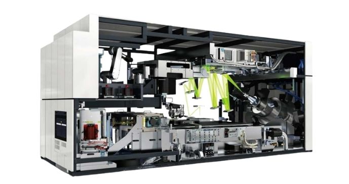
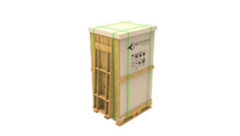
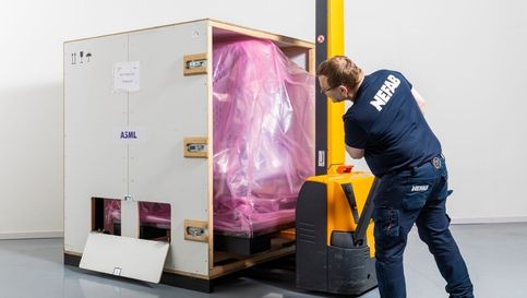
Semiconductor capital equipment and precision assemblies often require complex transport planning, clean handling, and strong protection against shock, vibration, and handling damage. When moving high-value manufacturing equipment, even small transit impacts can affect alignment, performance, or installation readiness. Protective packaging should be engineered to support product stability, handling, and transport requirements across domestic and global supply chains.
Nefab develops protective packaging solutions for semiconductor capital equipment and precision assemblies to help reduce transport risk, support clean handling, and improve operational readiness at destination.
Typical applications include:
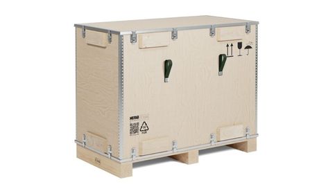
Our plywood based solutions are often combined with steel profiles, which creates a very rigid, strong but still lightweight solution. In addition, our plywood solutions are nail-free, which helps to create a safer, quieter work environment.
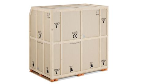
Nefab offers wood-based crating solutions for one-way and returnable semiconductor equipment flows. These solutions are designed to support product protection, handling efficiency, and reliable performance across complex logistics operations.
Corrugated is the most widely used packaging material in the industry. This is due in large part to its low cost, light weight and ease of use.
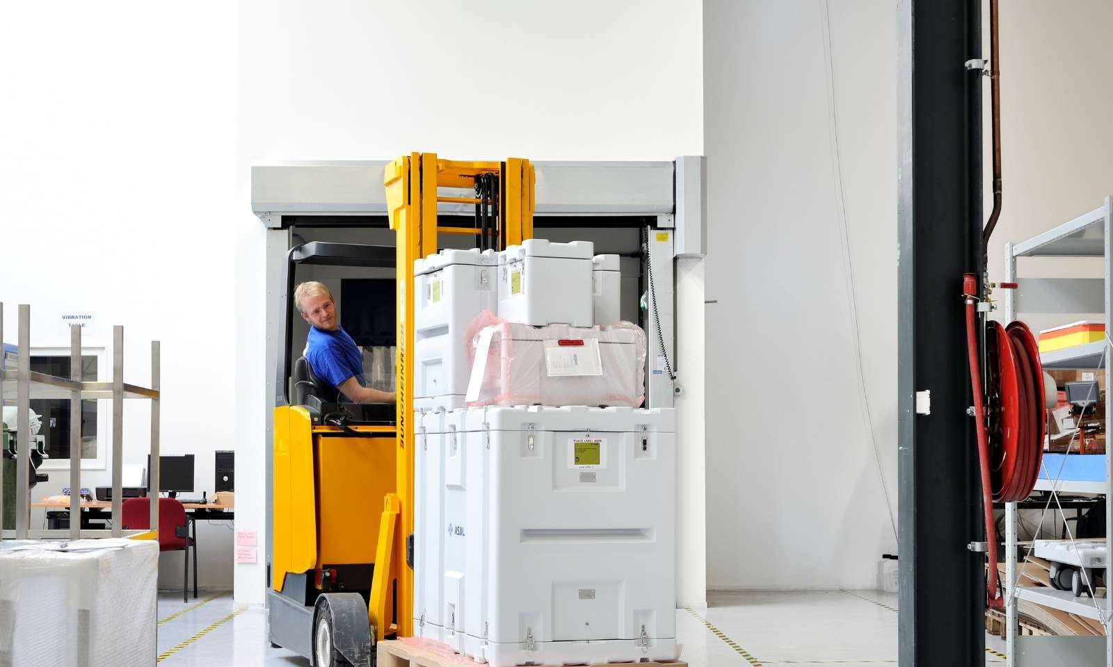
Nefab offers on-site packing services tailored to customer requirements, supporting safe packing and loading at customer facilities, warehouses, or other designated locations.

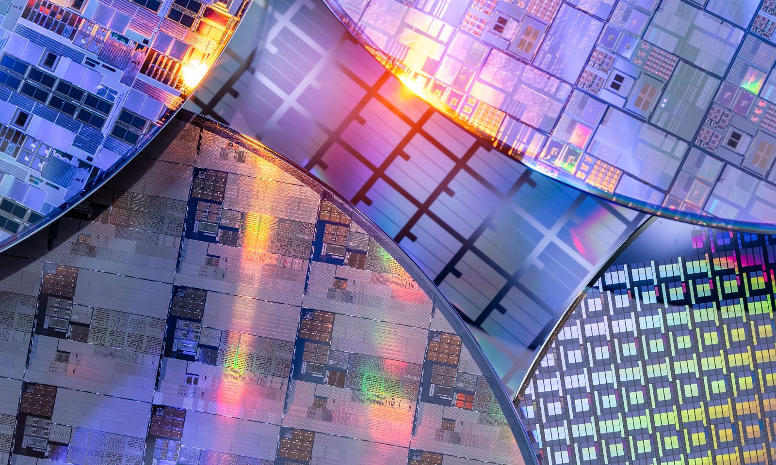
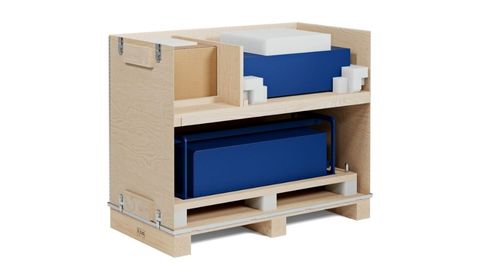
Semiconductor components, tools, and wafers often move through recurring logistics flows where cleanliness, handling consistency, and product protection are critical. These products may be sensitive to particle contamination, electrostatic discharge, and physical damage during storage, transport, and internal handling. Protective packaging should be designed to support repeatable flows, efficient handling, and reliable protection for sensitive parts.
Nefab develops protective packaging solutions for semiconductor components, tools, and wafers to help reduce contamination risk, protect sensitive products, and improve efficiency across recurring logistics operations.
Typical applications include:
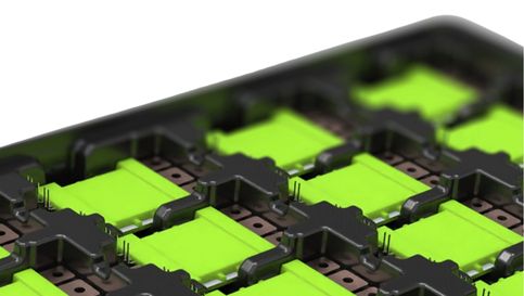
We offer several types of plastic solutions including clamshell wafer protection, ESD trays, and blisters to ensure that we can help you no matter the product that you are shipping.
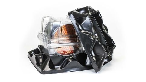
Packaging for wafers and sensitive components must protect against handling damage while supporting operational efficiency. Nefab offers custom thermoformed solutions designed for reliable protection, repeatable handling, and efficient logistics flows.
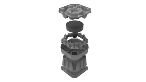
For electrostatic-sensitive and contamination-sensitive products, packaging design and material selection are critical. Nefab offers Reflex cushioning solutions developed to support clean handling and reliable protection for sensitive semiconductor applications.

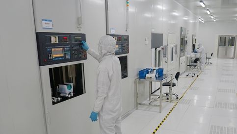
Semiconductor products used in cleanroom environments require packaging solutions that support contamination control, clean handling, and consistent performance throughout transport and storage. When products move between cleanrooms, production sites, or controlled environments, packaging must help maintain product integrity while supporting operational efficiency. Protective packaging should be designed to align with cleanliness requirements and controlled handling processes.
Nefab develops cleanroom-compatible packaging and transport solutions to help reduce contamination risk, protect sensitive products, and support reliable movement across cleanroom-related operations.
Typical applications include:
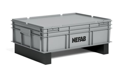
Transport Totes feature custom interior packaging for secure transport and storage. Tailored specifically for cleanrooms, they deliver reliable protection while minimizing contamination risks across your sensitive operations.
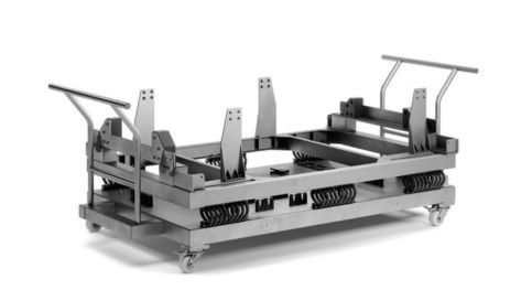
Safely transport high-value semiconductor equipment with our customizable transport assemblies. We build these precise handling solutions to your exact needs while ensuring full compliance with ISO Class 5-7 cleanroom standards.
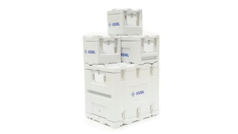
Streamline your cleanroom logistics with the innovative C2C Cube. Designed to maintain product integrity between cleanrooms, it also helps reduce waste through being a modular and returnable system. Equipped with integrated sensors, the C2C Cube provides real-time visibility, ensuring efficient and reliable operations.

We provide thorough cleaning services for the C2C cube, ensuring it meets top cleanliness standards. The cube can be cleaned, inspected, and prepared in our ISO class 5 and 7 cleanroom or at the customer's cleanroom if preferred.

In semiconductor supply chains, packaging is not a secondary concern. It directly affects product integrity, operational efficiency, and risk exposure across transport, handling, and cleanroom-adjacent environments. Nefab combines engineering, testing capabilities, and a global footprint to help customers turn packaging into a strategic advantage.
Semiconductor logistics often require more than basic protection. Nefab supports customers with packaging solutions and services designed for contamination-sensitive handling, cleanroom requirements, and operational consistency.
Packaging performance is increasingly evaluated not only by protection, but by cost efficiency and environmental impact. Using GreenCalc™ Life Cycle Analysis, Nefab helps customers quantify improvement opportunities and support more informed packaging decisions.
Semiconductor equipment, precision assemblies, and wafer-related flows demand packaging solutions designed around sensitivity, complexity, and performance under real-world logistics conditions. Nefab develops custom solutions tailored to product dimensions, fragility, cleanliness requirements, and transport risk.

Ewa Rosinek
Global Segment Director Semiconductors
Join us in transforming the future of semiconductor packaging. Contact us today to find out how our bespoke solutions can add value to your logistic needs and contribute to a sustainable footprint within the industry.
Write your future in clean, sustainable, and efficient packaging -- With Nefab, you're covered on all fronts.
Semiconductor manufacturing leaves no room for error. Yet, shipping high-value parts such as electrostatic chucks, pedestals, or showerheads introduces a whole new layer of risk.

The semiconductor industry is entering one of the most transformative decades in its history.

The semiconductor equipment industry is no stranger to innovation, yet sustainability is becoming an increasingly urgent matter.