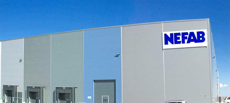
“Our operations in Romania started in the Autumn of 2006. Since then, we have grown our business, added new projects and new partners. In order to support the dynamic of day to day operations, understanding and even anticipating our customer’s needs – in terms of products, support, services – we have taken a new step in our company development, so 9 years later – Autumn 2015 we have kicked off the new establishment, located near Timisoara, in Ghiroda." says Managing Director, Valentin Cica.
The new facility consist of roughly 500sqm of warehouse, own operated, 1000+sqm production and 300sqm(on two floors) offices.
Here we convert foams, corrugated plastic and paper, assembly and kitting multiple other materials into CPS(complete packaging solutions).
By adding a modern and performant 3D plotter, we have a great support for our engineers during development and testing new concepts and prototypes, then shortening the time to introduce the new projects. The flexibility – of smaller batches – increased, due to capabilities of this new equipment.
From logistic perspective, we benefit by proximity to the highway, so “we are closer to our customers"
The whole team look forward to serve our customers with even higher enthusiasm and we are welcoming all of you to visit us!”