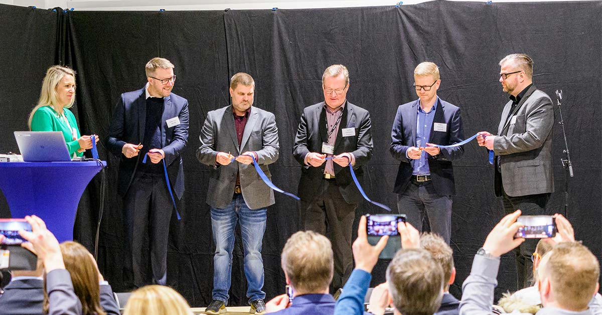
Yesterday we gathered customers and partners to inaugurate our new warehouse facility in Tampere, Finland. We are proud to strengthen our capabilities by adding another location to our operations.
We want to thank our team in Finland and all participants for making this a great event! We would also like to send our best wishes to our team in Finland.