• Corporate News

Nefab Expands its North American Footprint

So far, we have added three new sites in the US this year.

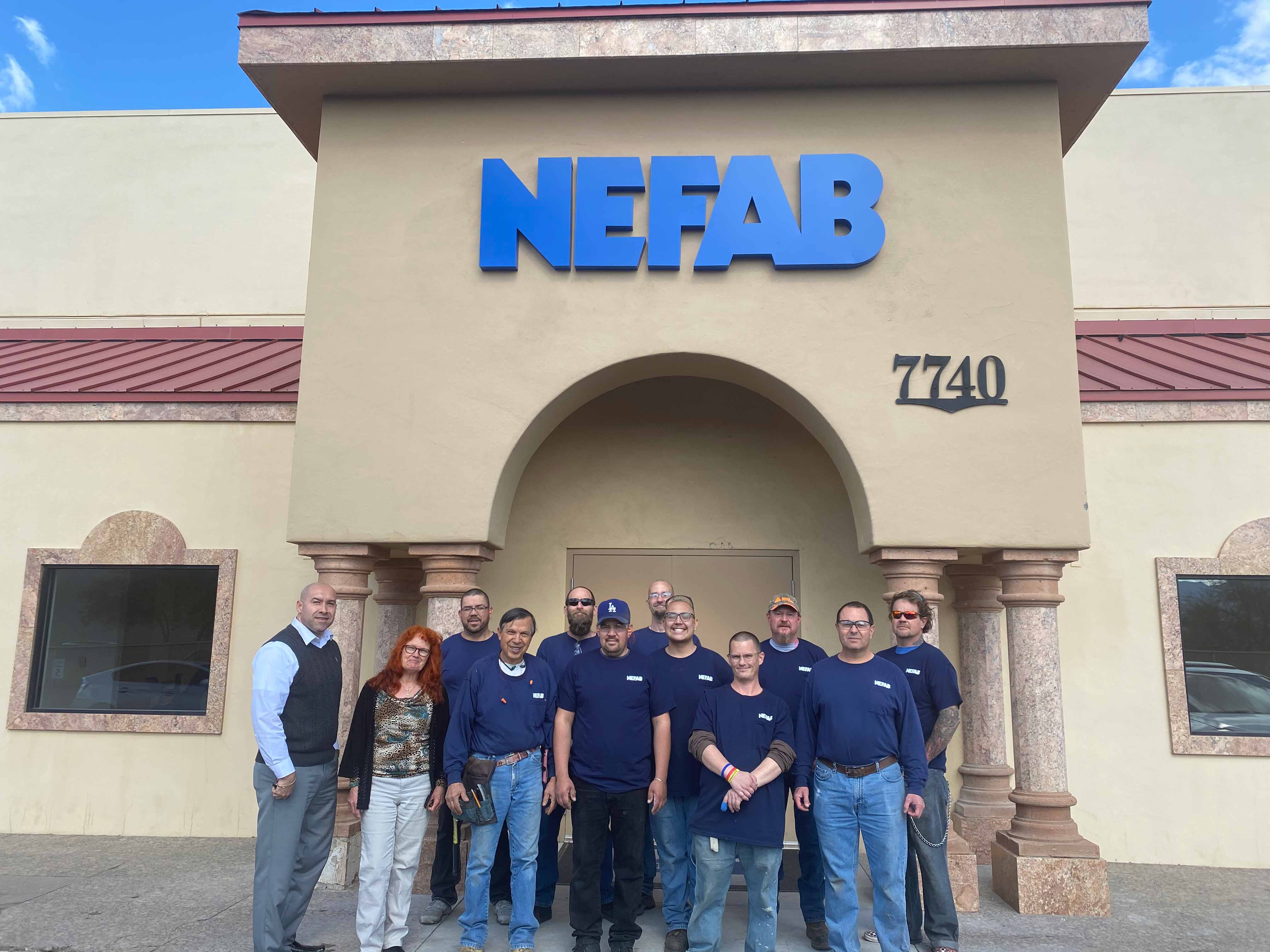
This year, we have added sites in Houston, TX, Tucson, AZ and Gainesville, FL, and they have each been instrumental in supporting our customers' ambitions in their respective regions. A big thank you to our new teams for all the hard work!

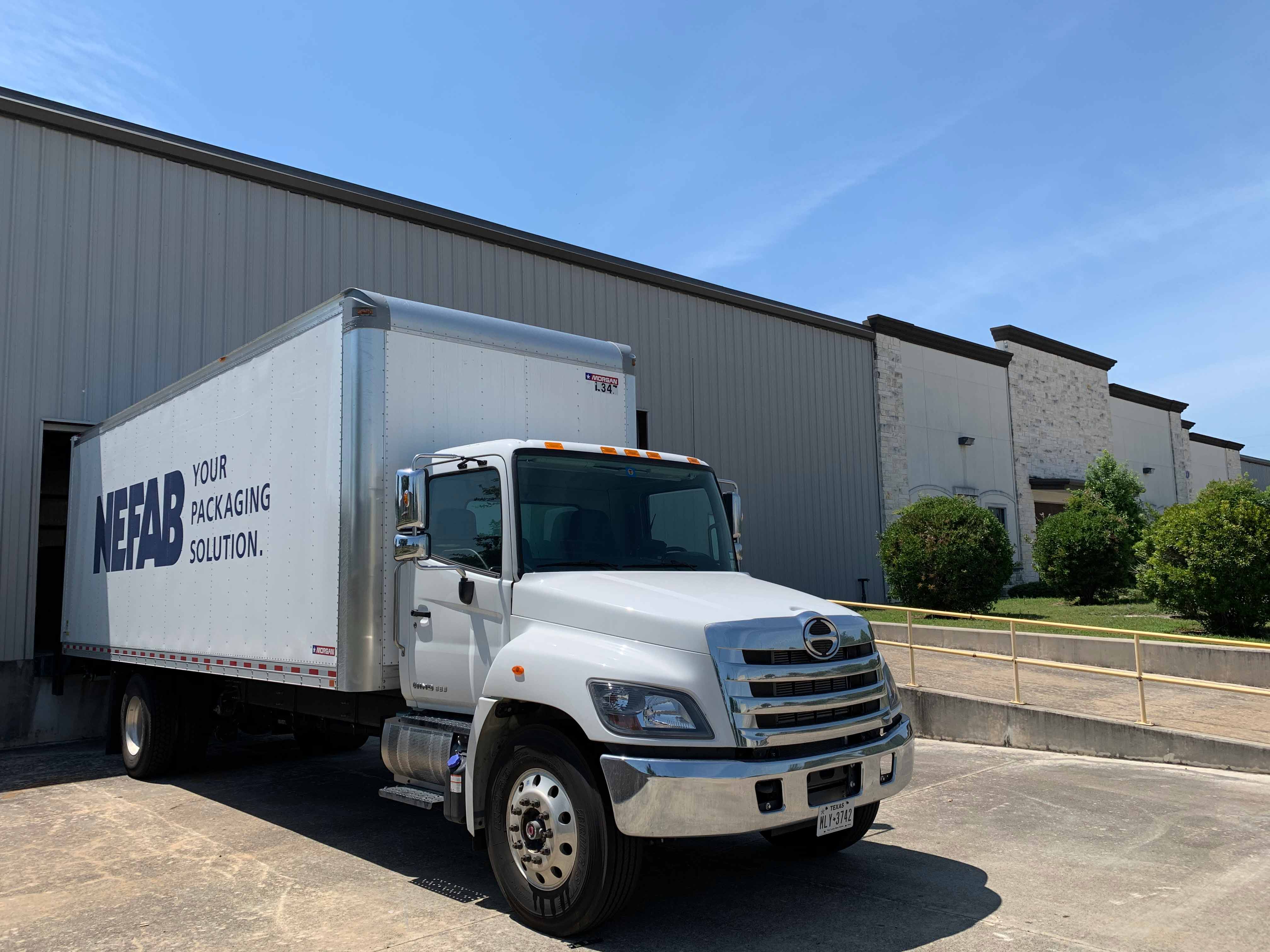
With a growing presence in North America and around the world, we can provide the solutions and services you need, no matter where you are.


Are you in any of these areas? Contact us today to see how we can help with your packaging needs!


Our latest news & insights
  • 2025.12.02 Semiconductor

    How to Protect Semiconductor Manufacturing Equipment in Transit?

    Semiconductor manufacturing leaves no room for error. Every process, every component, every piece of equipment operates within microscopic tolerances, and that precision can’t be compromised once the machines leave the cleanroom. Yet, shipping high-value parts such as electrostatic chucks, pedestals, or showerheads introduces a whole new layer of risk.

  • 2025.11.26 Customer Cases

    Sustainable Packaging for Wafer Shipping

    Semiconductor manufacturing is a complex process that can be broadly divided into two main phases: the front-end process and the back-end process. Nefab partnered with a leading semiconductor manufacturer to optimize the packaging solution for shipping wafers between its front-end and back-end facilities, achieving significant financial and environmental benefits.

  • 2025.11.25 Energy

    Why Shipping Grid Equipment Is a Different Kind of Challenge and How to Overcome It?

    Why Shipping Grid Equipment Is a Different Kind of Challenge and How to Overcome It?