- News & Insights
- 2023
- How can you ensure the safety of semiconductors during transportation with advanced packaging solutions?
- Semiconductor
- Industries
- Insights
News & Insights
Ensuring Safe Transport of Semiconductors
How can you ensure the safety of semiconductors during transportation with advanced packaging solutions?
Combining packaging expertise with semiconductor companies' individual challenges and requirements is pivotal in advancing the semiconductor industry's sustainability.
The manufacturing components and equipment utilized in the semiconductor industry are both delicate and costly. Given the ongoing market shortages, any mishaps in their transportation can result in significant delays and loss of revenue. As the supply chain becomes more complex, these components often pass through multiple stages of transportation before reaching their ultimate destination.
There needs to be more than a one-size-fits-all approach for safeguarding semiconductor production. To ensure their safe and reliable transportation, it is essential to develop packaging and logistic systems that are highly robust and tailored to specific needs and applications. Designing protective and sustainable packaging is possible through the cooperation between the technology and packaging engineers. All that with respect to the environment and sustainability principles in mind.
OPTIMIZED PACKAGING KEEPS THE INDUSTRY ON TRACK
The semiconductor market shortages have impacted many industries in the past few years. While the demand in sectors such as PCs or mobile phones might be cooling, the automotive industry’s semiconductor needs are growing exponentially. According to S&P Global Mobility, in 2021, production of over 9.5 million units of global light vehicles were lost because of a lack of semiconductors. Although the situation has improved since, with the losses falling to about 524,000 units globally during the first half of 2023, the semiconductor supply chain remains constrained1. With the lead time doubling compared to the pre-COVID-19 era2, unsettling uncertainty hangs over not only the automotive industry but also across a wide range of sectors across the globe.
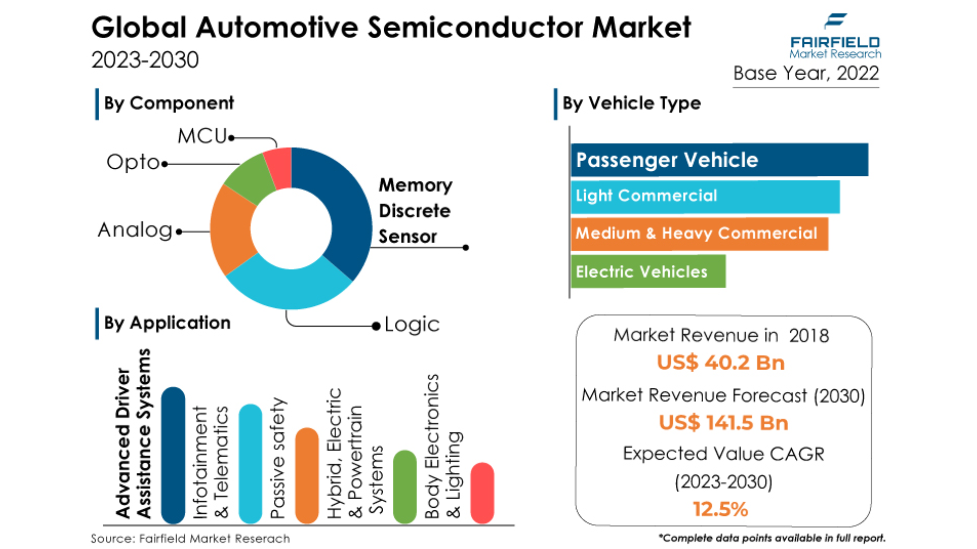 The global automotive semiconductor market is expected to achieve a revenue exceeding US$141 billion by the end of 2030 (source: Fairfield Market Research)
As the semiconductor market grapples with shortages and surging demand, there is zero tolerance for errors or damages during transit. Despite their small size, semiconductors are technological marvels, and their fragility and high production costs demand packaging solutions that go beyond the standard safety precautions. Each semiconductor component embarks on a complex journey before it finds its destination, and this expedition is fraught with numerous handling, environmental, and potential hazard-related challenges.
ADDRESSING INDIVIDUAL NEEDS
No company can achieve its objectives or overcome industry challenges in isolation. Collaboration is at the heart of this endeavor, so packaging needs should be considered at the New Product Introduction (NPI) stage. This cooperative approach emphasizes the significance of combining packaging expertise with semiconductor companies' individual challenges and stringent, sometimes unique requirements. The era of one-size-fits-all approaches is giving way to tailored packaging solutions that address specific needs in a constantly evolving industry.
Open dialogue and a clear understanding of semiconductor equipment manufacturers' challenges are critical. Through that, packaging suppliers can spot improvement opportunities, explore alternatives, and concentrate on what truly matters. What does this mean in practice? For instance, assessing permissible shipping orientations can substantially increase part loading density, resulting in lower shipping costs, reduced CO2-eq emissions per part, decreased shipping volume, and reduced storage space requirements. Sharing knowledge and developing solutions through cross-sectoral partnerships is pivotal in advancing the semiconductor industry's sustainability, particularly in transportation.
 Combining packaging expertise with semiconductor companies' individual challenges and requirements is pivotal in advancing the semiconductor industry's sustainability.
FOCUS ON TRACEABILITY
Packaging for semiconductor components plays a vital role in ensuring safe transportation by providing physical protection against shocks and impacts, maintaining controlled environmental conditions, preventing contamination (which we discussed here), securing containment, and enabling easy identification and traceability. Customized to meet specific component requirements, engineered packaging complies with industry standards and regulations and facilitates efficient handling, safeguarding these delicate and sensitive devices from various hazards encountered during transit.
At Nefab, we work together with many businesses in the semiconductor industry to champion new sustainable packaging solutions that optimize the supply chain and help them reach their sustainability goals. Get in touch to learn how we can support you.
We save resources in supply chains, for a better tomorrow.
Want to learn more?
GET IN TOUCH
Contact us to learn more about our smart and sustainable solutions.
LEARN MORE
GreenCALC
Nefab’s own certified calculator measures and quantifies financial and environmental savings in our solutions
Sustainable Solutions
Engineered packaging for sustainable supply chains
Sustainable Materials
Fiber-based packaging and raw materials