- News & Insights
- 2023
- Rethinking plastics consumption in the Semiconductor Industry through Innovative Packaging Solutions
- Semiconductor
- Industries
- Insights
News & Insight
Semiconductor Industry
Rethinking plastics consumption through innovative packaging solutions
The semiconductor industry's relentless pursuit of smaller, faster, and more efficient technology has transformed the way we live, work, and connect.
The semiconductor industry's relentless pursuit of smaller, faster, and more efficient technology has transformed the way we live, work, and connect. However, as the demand for cutting-edge electronics continues to soar, so does the industry's reliance on plastic packaging, which poses a significant sustainability dilemma. It's a conundrum that calls for a paradigm shift, a transformation of not only the products themselves but also the very materials that protect and transport them. What if we could reimagine the very foundation of this packaging, infusing it with sustainability without compromising on performance or functionality?
Follow along as we explore a groundbreaking solution that promises to revolutionize the industry's approach to packaging – recyclable thermoformed trays. These trays, born from the crucible of sustainability and precision engineering, offer a glimmer of hope in the quest to reduce plastic consumption without compromising the integrity of high-tech components.
Sustainability & Cleanliness
The recent rise in the use of thermoformed plastic packaging for semiconductors is not without reason. In fact, thermoformed plastic trays answer both the need for sustainability and cleanliness. Produced from 100% recycled post-consumer HDPE, they are easier to recycle and reuse in return and circular flows compared to standard plastics, thus contributing to creating a truly circular plastic loop.
Besides their reusability and recyclability, thermoformed trays offer cleaner performance than standard foams. On top of that, by using reusable thermoformed trays every company can significantly reduce their CO2 emission, even up to 70%. Another key benefit is flexibility as thermoformed solutions can be used to pack many commonly used components in semiconductor manufacturing, such as pedestals, showerheads, electro-static chucks (ESCs), ceramic rings and wafer shipping boxes.
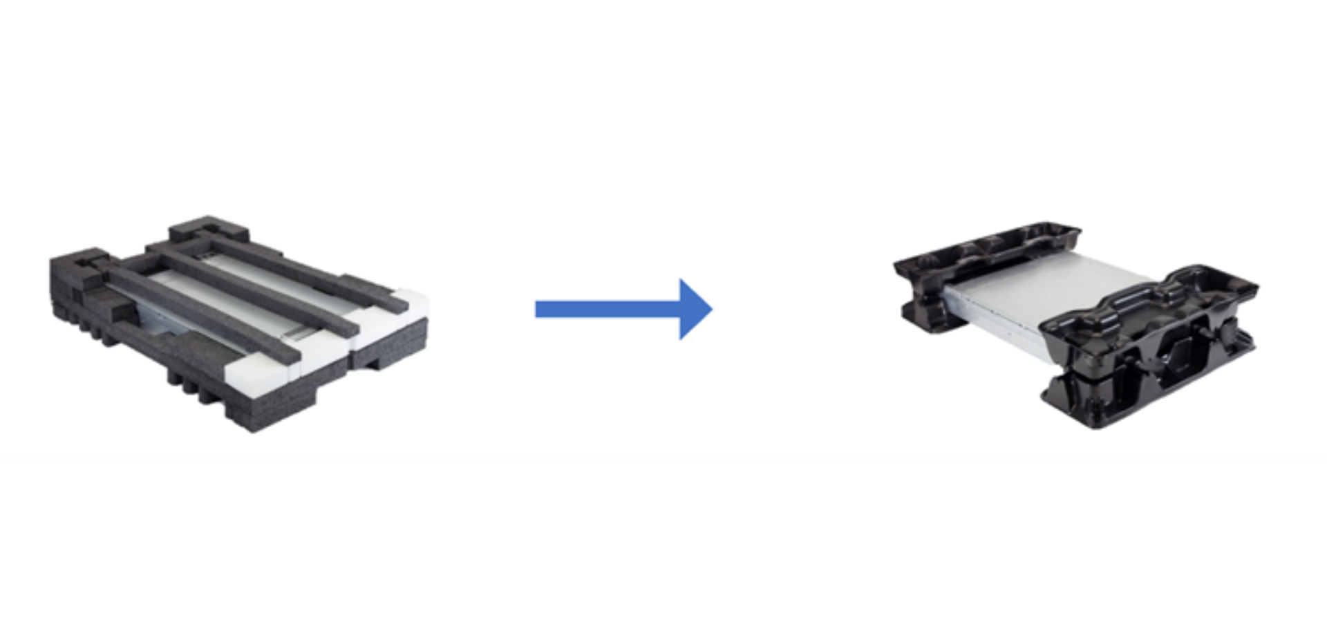
 Nefab thermoformed cushion designs for semiconductor components allow to save 85% of space during inbound transport and supply base storage.
Cost-effective and recyclable
What is more important, thermoformed packaging solutions are more nestable than standard PE foam which allows to save up to 85% of space during inbound transport and supply base storage. Not to mention they are more cost effective as their price is up to 30% lower than PE foams.
Last, but not least, the results can be measured and quantified with Nefab’s own environmental calculator tool GreenCalc, which is impartially ISO certified and integrated with SIMAPro. Additionally, Nefab offers more than just analysis of the process; the company utilizes the circularity of thermoformed plastics. Customers’ thermoformed waste can be collected, cleaned, shredded, and extruded for reuse as raw material for new products. This keeps the plastics in circular use, which reduces costs and CO2 emissions in customers’ supply chains. As a result, these recycled thermoformed trays are a perfect fit for return and circular flows, making supply chains more sustainable (read more here).
Closing the loop for better tomorrow
By switching from traditional foam-based packaging to thermoformed plastic solutions, semiconductor manufacturers can contribute to significantly reducing scope 3 emissions. At Nefab we work together with many businesses to champion new sustainable packaging solutions that optimize the supply chain and help them reach their sustainable goals. Get in touch to learn how we can support you.
We save resources in supply chains, for a better tomorrow.
Want to learn more?
GET IN TOUCH
Contact us to learn more about our smart and sustainable solutions.
LEARN MORE
GreenCALC
Nefab’s own certified calculator measures and quantifies financial and environmental savings in our solutions
Sustainable Solutions
Engineered packaging for sustainable supply chains
Sustainable Materials
Fiber-based packaging and raw materials
