• Corporate News

Nefab Engineering Center Silicon Valley

To serve the growing needs of our customers in the Data and Telecom industry Nefab has expanded its capabilities in the Northern California facility to include a state of the art engineering and testing center.

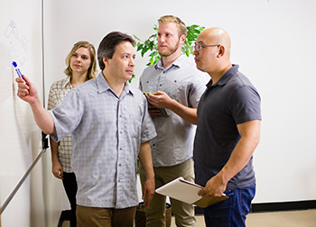
In one location we combine engineering, prototyping, testing, scientific evaluation and production to offer our customers and datacom companies a fast and seamless development to market process for their packaging requirements. Our in-house lab delivers immediate results from testing, which provides feedback, and offers brainstorming opportunities, to develop innovative packaging solutions.

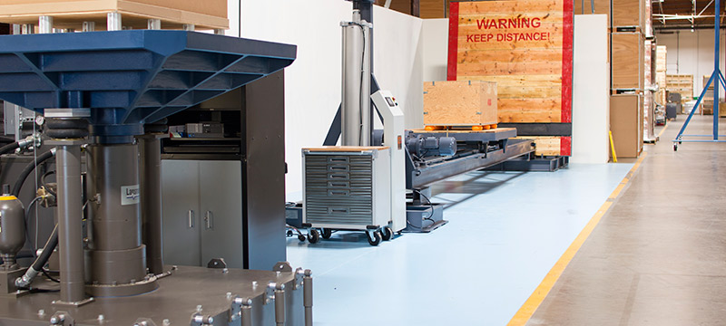
The new lab offers state of the art testing equipment for all packaging components, including a vibration table, compression tester, incline impact tester, climate chamber, large and small drop tester, as well as a variety of material testers where we can qualify and review materials from all over the world. The test lab will be ISTA certified by the end of the year.

The Datacom (Cloud) industry requires product and product packaging to meet short deadlines, limited product life cycles, and multifaceted development phases. Our building has a full suite of capabilities starting with design, testing, samples, small to large run fabrication and JIT services to meet a market heavy in R&D yet with customers who are capable of large run production. The goal is to be a “one stop shop” servicing local needs with an eye to develop the customers global needs in mass production countries. 


Our packaging team in Silicon Valley includes six engineers with extensive global expertise on material and design development. The possibility to test materials from all over the world ensure that US based development and design will have no impact when it comes to local availability of equivalent global materials. Together with our global EDM system for drawings, we can assure easy transaction between countries and regions as products and production move from one location to the other. Lastly, our market is trending rapidly towards green, smarter packaging. Our team in Silicon Valley is committed to making a difference with sustainable packaging in efforts to be Best in Class as we innovate new products.
Our latest news & insights
  • 2025.12.02 Semiconductor

    How to Protect Semiconductor Manufacturing Equipment in Transit?

    Semiconductor manufacturing leaves no room for error. Every process, every component, every piece of equipment operates within microscopic tolerances, and that precision can’t be compromised once the machines leave the cleanroom. Yet, shipping high-value parts such as electrostatic chucks, pedestals, or showerheads introduces a whole new layer of risk.

  • 2025.11.26 Customer Cases

    Sustainable Packaging for Wafer Shipping

    Semiconductor manufacturing is a complex process that can be broadly divided into two main phases: the front-end process and the back-end process. Nefab partnered with a leading semiconductor manufacturer to optimize the packaging solution for shipping wafers between its front-end and back-end facilities, achieving significant financial and environmental benefits.

  • 2025.11.25 Energy

    Why Shipping Grid Equipment Is a Different Kind of Challenge and How to Overcome It?

    Why Shipping Grid Equipment Is a Different Kind of Challenge and How to Overcome It?