- News & Insights
- 2023
- Advancing Safety and Quality in Semiconductor Industry Cleanrooms through Sustainable Thermoformed Packaging Solutions
- Semiconductor
- Industries
- Insights
News & Insights
Advancing Safety and Quality in Cleanrooms
Advancing Safety and Quality in Semiconductor Industry Cleanrooms Through Sustainable Thermoformed Solutions
Discover how innovative thermoformed packaging solutions help semiconductor manufacturers boost cleanroom safety, reduce contamination, and achieve greater sustainability—all while supporting industry growth.
The semiconductor market has experienced rapid growth in recent years. With rising demand, the market is expected to become a trillion-dollar industry by 20301. However, for the market to keep thriving, the semiconductor manufacturers must switch to more sustainable packaging materials to limit their emissions and increase safety and quality of their cleanroom environment.
To ensure the highest levels of quality, safety and repeatability in the chips, semiconductor manufacturers must carry out the processes in a controlled environment. That’s why packing semiconductor components cleanly is critical for the final product's performance. At the same time, the semiconductor market is very cost-sensitive and demanding in terms of process automation. Fortunately, the standardized or custom thermoformed solutions can provide a solution in both cases. Keep reading to discover how sustainable cleanroom packaging solutions can help answer the biggest threats to semiconductor manufacturing.
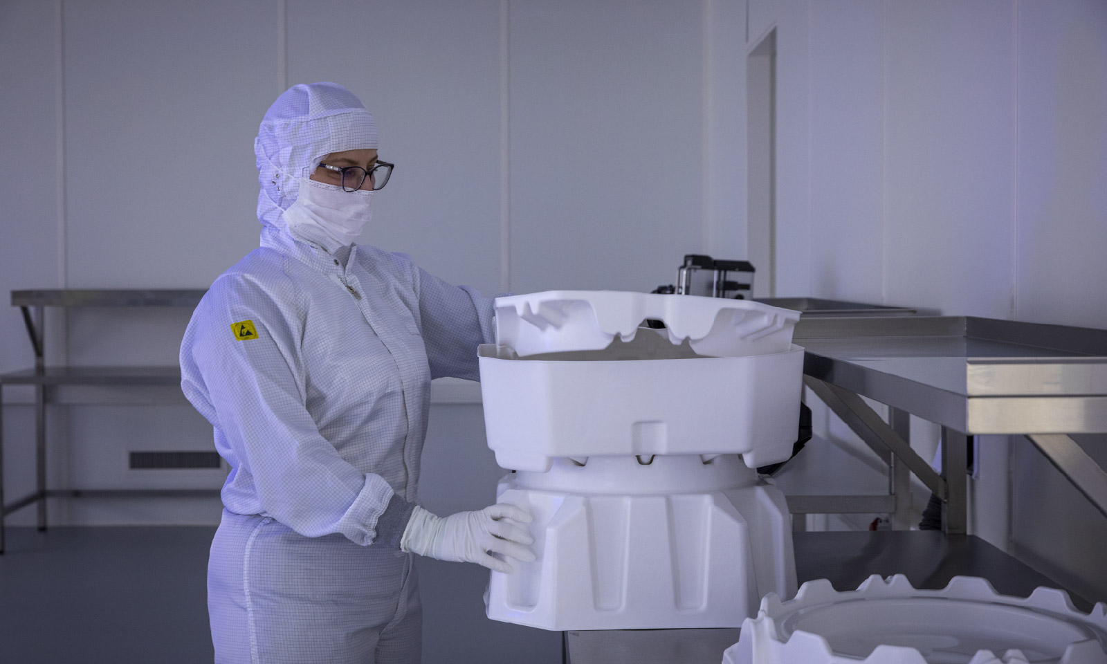 The smooth surface of thermoformed cushions prevents build-up of particles and allows easier cleaning than the packaging made from regular PE foam.
The Challenging Road to Safe Semiconductor Manufacturing
Particulate matter, electrostatic discharge (ESD), humidity, and outgassing are four of the biggest threats to semiconductor manufacturing, even in controlled cleanroom environments2. Just like with any other cleanroom products, airborne particles like dust, viruses, and bacteria, along with human contamination, are the factors most difficult to control. Despite wearing the protective cleanroom clothing, particulate build-up poses a substantial risk to semiconductor applications. Static, on the other hand, corrupts materials by drawing and adhering fine airborne particulates to the products’ surface, ultimately resulting in silicon wafers defects or failure, and in rare cases, it can even cause electric shocks to operators.
Another crucial factor to consider is fluctuating humidity and temperature levels which can affect cleanroom productivity and quality. From inconsistent bake-out times to evaporation of solvents to surface swelling and corrosion, any inconsistency in the approved temperature (ca. 70ºF) can end up in product failure. Last, but not least, outgassing is another common concern with electronic equipment. Although the release of the gas that was trapped or stored within in a solid material is not possible to be eliminated, it should be prevented and controlled as much as possible during the product manufacturing phase.
Enhanced Safety and Cleanliness of Thermoformed Solutions
That’s where thermoformed packaging solutions come into play. Thanks to their smooth surface they are much easier to clean than PE foam. They also successfully block electro-static discharge thanks to special ESD-properties which reduce particle attraction.
Key benefits of thermoformed solutions include:
- Reduced Particle Shedding: Compared to PE foams, the smooth surfaces of thermoformed trays offer significantly lower particle shedding.
- Reusability and Recyclability: Designed from up to 100% recycled post-consumer HDPE, they are easier to recycle and reuse in return and circular flows.
- Lower CO2 eq Emissions: Their nestable character allows for savings of up to 85% of space during inbound transport and storage, significantly reducing carbon dioxide equivalent (CO2 eq ) emissions.
By using thermoformed trays, companies can contribute to creating a truly circular plastic loop while improving their environmental footprint.
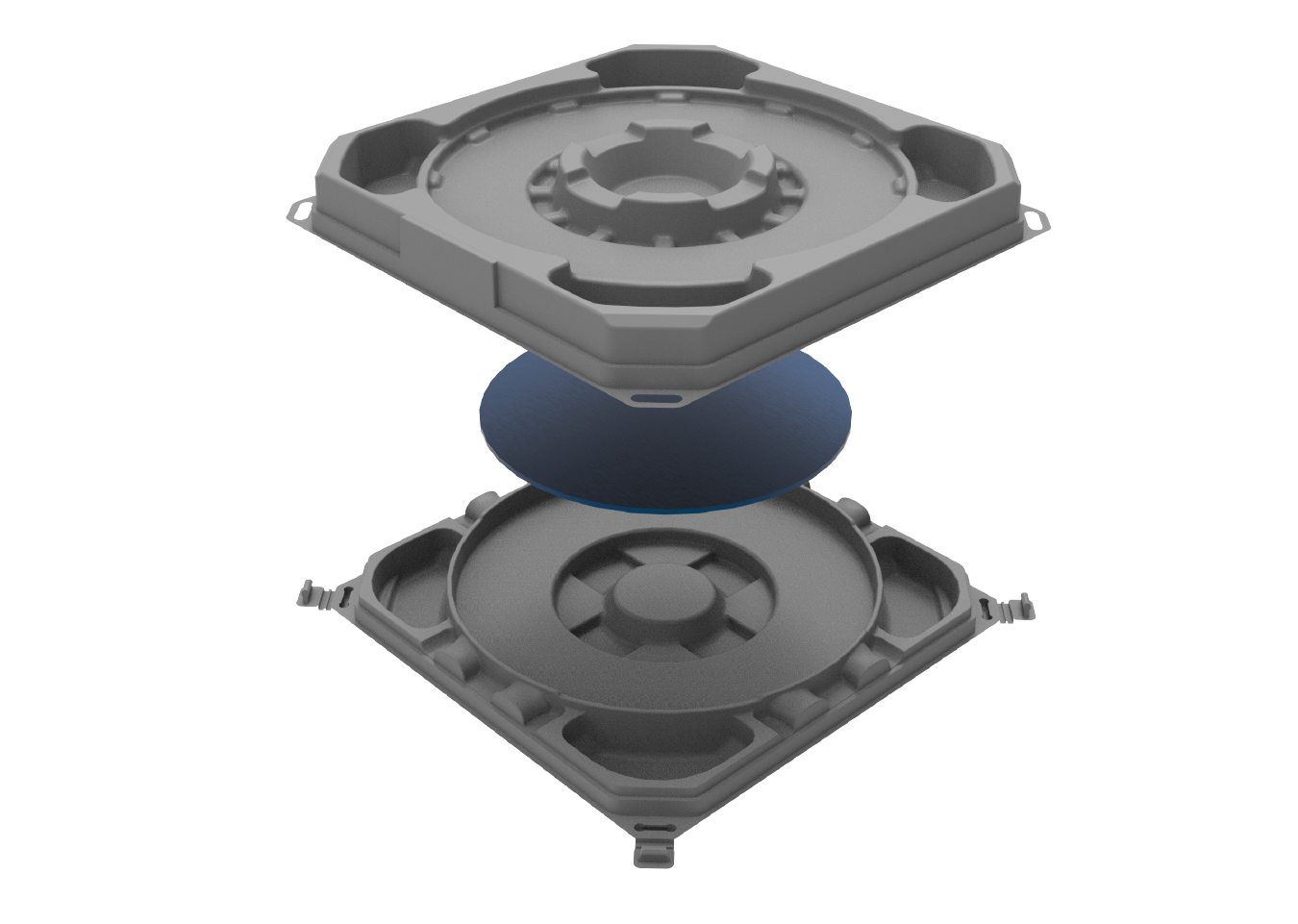 Nefab thermoformed cushion designs for semiconductor components.
Answering Rising Demands with Safety in Mind
The good news is that semiconductor companies can achieve safety and quality in cleanroom environment through various means, from improving manufacturing processes and using more energy-efficient equipment to switching to more sustainable packaging materials. Innovative thermoformed packaging solutions, made from recycled post-consumer waste, are playing a crucial role in answering the biggest threats to safe semiconductor manufacturing. By leveraging these solutions, semiconductor companies can make significant strides in reducing their environmental impact while maintaining high industry standards.
At Nefab we work with many businesses to champion new sustainable cleanroom solutions that optimize the supply chain and help them reach their sustainable goals. Get in touch to learn how we can support you.
Frequently Asked Questions
How does thermoformed packaging improve cleanroom safety?
Its smooth, low-shedding surface minimizes particle contamination. Special ESD properties also reduce the risk of electrostatic discharge, protecting sensitive components.
Are thermoformed trays a sustainable packaging option?
Yes. They are made from 100% recycled post-consumer HDPE, designed for reuse in circular flows, and are easily recyclable, which helps reduce waste and CO2e emissions.
Want to learn more?
GET IN TOUCH
Contact us to learn more about our sustainable solutions.
LEARN MORE
GreenCALC
Nefab’s own certified calculator measures and quantifies financial and environmental savings in our solutions
Sustainable Solutions
Engineered packaging for sustainable supply chains
Solutions for the Semiconductor Industry
Engineered for precision and sustainability
Cover image: Adobe Stock