News & Insights
Nefab earns sixth ISTA Test Lab Certification in Taiwan
We're thrilled to announce that Nefab’s test lab in Taoyuan, Taiwan has earned a certification from the International Safe Transit Association (ISTA)
This exciting milestone expands Nefab’s global footprint from five to six ISTA certified test labs worldwide, with skilled multi-material packaging engineers across the Americas, Asia, and Europe, demonstrating our commitment to high performance packaging solutions.
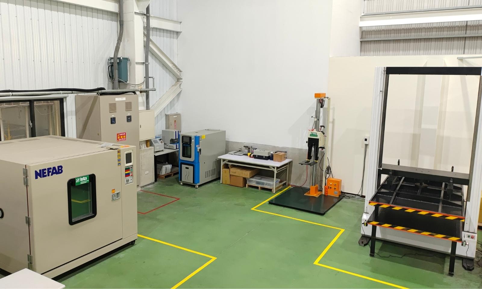
Our ISTA certified lab in Taoyuan is equipped with state-of-the-art testing equipment designed to simulate a variety of transportation environments. These include conditions such as vibration, shock, drop, compression, and temperature – all critical factors that can affect the integrity of packaging during transit. In cases where physical testing may not be possible, we employ Finite Element Analysis (FEA) to verify packaging solutions, demonstrating our adaptability and commitment to thorough testing under all circumstances.
"This certification not only validates our capabilities and commitment to excellence, but it also underlines our growth as a global leader in packaging solutions. It's a proud moment for all of us at Nefab Taiwan, and it wouldn't have been possible without the dedicated efforts of our team"
Jacob Liao, Managing Director, TaiwanBehind the advanced technology at our Taoyuan lab is a team of dedicated engineers, committed to ensuring the highest level of service and quality. They will work with you to develop a customized testing plan that meets your specific requirements. Once testing is complete, we will provide you with detailed reports that include all necessary data and analysis to help you make informed decisions about your packaging.
Contact us today to discover more about how Nefab's ISTA Lab in Taoyuan, Taiwan can contribute to your packaging success. Join us on this journey of innovation and excellence in industrial packaging solutions.