- News & Insights
- 2025
- Accelerated Packaging Design for Datacom and Cloud Demand
- Datacom and Cloud
- Industries
- Insights
Accelerated Packaging Design for Datacom and Cloud Demands
How Accelerated Packaging Design is Helping Datacom and Cloud Companies Keep Up with Global Infrastructure Demand
In today’s AI-powered world, every second counts, and for datacom and cloud infrastructure leaders, time lost is opportunity lost. As demand for data skyrockets, so does the need for faster, more efficient infrastructure. The rise of generative AI and cloud computing has pushed data center growth into overdrive. Global data center capacity is expected to grow at 15% annually, yet even that may fall short of meeting future demand 1.
In this high-pressure environment, delays come at a high cost. Today’s supply chains are under more pressure than ever, and trade, economic, and geopolitical challenges only add to the complexity2. To keep up, companies are regionalizing data center deployment and beefing up their risk management strategies3. Today, agility and safety are essential. Every component, from servers to cooling systems, must arrive on time and in perfect condition. Amid all this complexity, one often-overlooked factor can make or break the timeline: packaging.
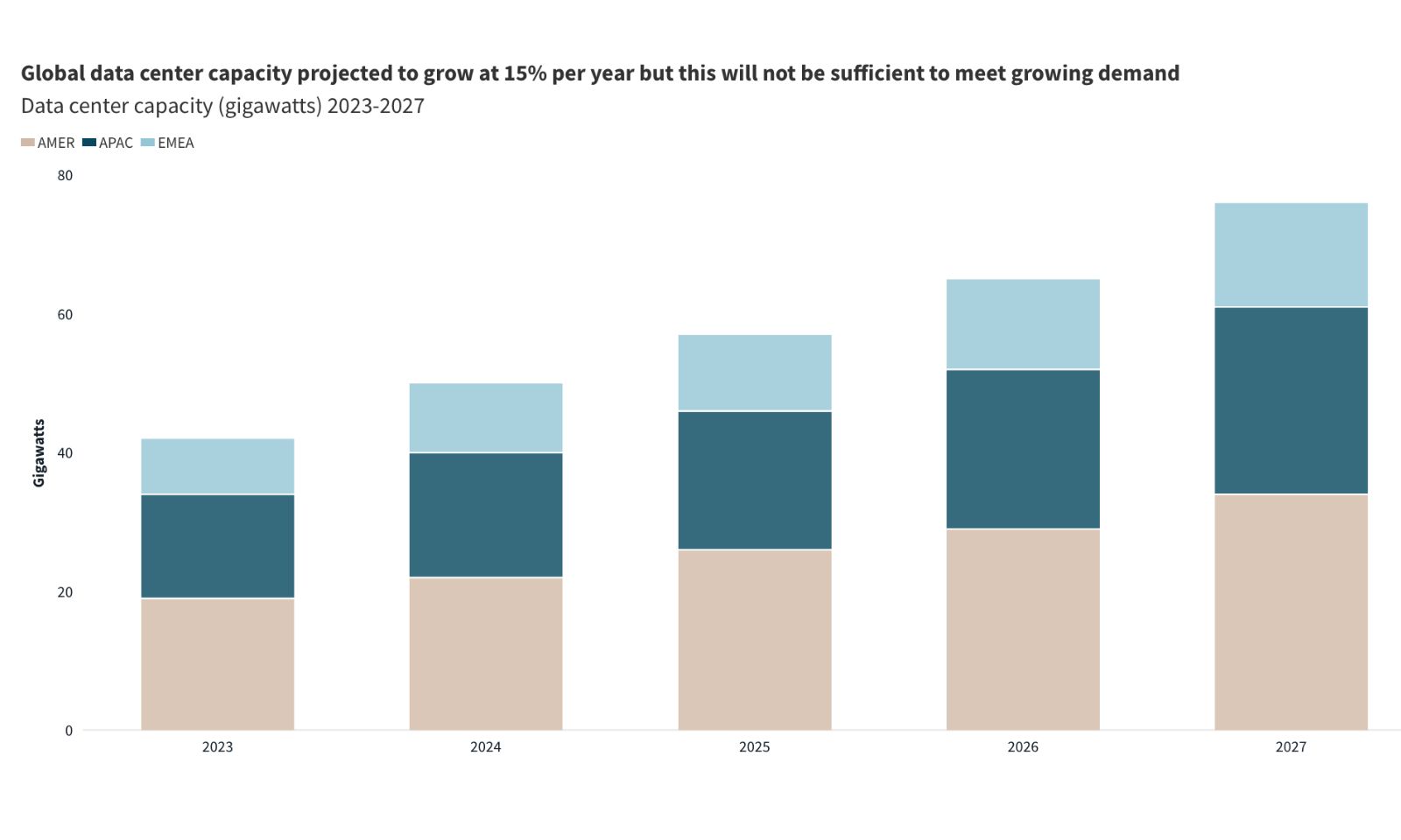
Even as global data center capacity increases at a rate of 15% per year, experts warn this may still fall behind accelerating demand. Source: 2025 Global Data Center Outlook by JLL
Why Packaging Is Key to Datacom and Cloud Infrastructure Growth
Packaging can be a bottleneck or a competitive advantage in this race for speed and efficiency. Yet it’s too often treated as an afterthought, despite its critical role in avoiding costly delays and ensuring consistent performance across global markets. The ability to move from concept to delivery at record speed depends not only on production capacities, but also on packaging solutions that are agile, compliant, and globally scalable.
In the datacom and cloud industry, we’re under constant pressure to deliver faster, with fewer disruptions. When packaging is developed in silos, it slows everything down. Bringing design, testing, and production together under one roof has been a game-changer. It gives our customers the speed and reliability their supply chains depend on.
Todd Novitske, Segment Director Datacom and Cloud at NefabWhy Integrating Design, Prototyping, and Testing Matters
To meet infrastructure demands and stay ahead of market pressures, datacom and cloud industry leaders are embracing a one-stop-shop approach, bringing packaging design, prototyping, and testing under one roof.
Streamlined Design
Optimizing packaging design focuses on minimizing material use without compromising protection. Modular designs are particularly valuable, as they can be easily adapted to different regional requirements while maintaining speed and efficiency.
Rapid Prototyping for Immediate Feedback
By centralizing design and prototyping, companies gain the availability to revise the concepts quickly and test ideas in real time. Digital tools enable rapid adjustment, shortening development cycles and reducing the risk of delays caused by back-and-forth with multiple suppliers.
Testing for Reliability: In-Lab vs Virtual
In-lab testing remains crucial in some cases (e.g. regulatory compliance), but virtual testing offers a faster, more flexible way to simulate real-world scenarios - especially in situations where physical testing isn’t possible (as discussed further in this article).

Future-oriented companies are integrating packaging early in the design process to reduce risk, accelerate timelines, and ensure consistent quality across markets.
The Competitive Edge of a One-Stop-Shop Packaging Strategy
A fully integrated packaging approach delivers several key advantages in today’s datacom and cloud industry ecosystem:
- Speed: By working with one supplier, companies can iterate faster and shorten time to market.
- Cost Efficiency: Optimized designs and fewer material changes drive down costs.
- Consistency: Standardized solutions ensure the same protection, quality, and compliance across all regions.
- Data-driven decisions: With digital tools, immediate feedback on packaging performance enables continuous optimization based real-word data.
These benefits aren’t just theoretical, they’re playing out in real time across the industry.
With over 75 years of experience and a powerful hub of 250+ engineers and 6 ISTA certified labs, Nefab can support companies worldwide.
Rethinking Packaging as a Strategic Asset
As digital infrastructure grows faster, datacom and cloud companies are rethinking where delays can be reduced, and packaging is part of the answer. When integrated early, it can boost speed, reduce risk, and help teams adapt to changing demands. Reframing packaging as a core element of new product launches or infrastructure deployment could be the edge that sets tomorrow’s frontrunners apart.
We save resources in supply chains, for a better tomorrow.
Want to learn more?
GET IN TOUCH
Contact us to learn more about our sustainable solutions driving supply chains forward.
LEARN MORE
Solutions for the Datacom and Cloud Industry
Unmatched expertise in Datacom and Cloud supply chain excellence
GreenCalc
Nefab’s own certified calculator measures and quantifies financial and environmental savings in our solutions
Global Supply & Local Services
With over 250 engineers across more than 130 locations, working together in a global network, you can count on us for your next packaging project.