As geopolitical tensions, demand for advanced chips, and national self-sufficiency strategies reshape global production, manufacturers are investing heavily in regionalized, resilient supply chains.
By 2030, the industry is expected to invest over $1 trillion in new semiconductor fabs1 . While the growth prospects are huge, manufacturers are also facing serious challenges that make cost efficiency and sustainability more critical than ever.
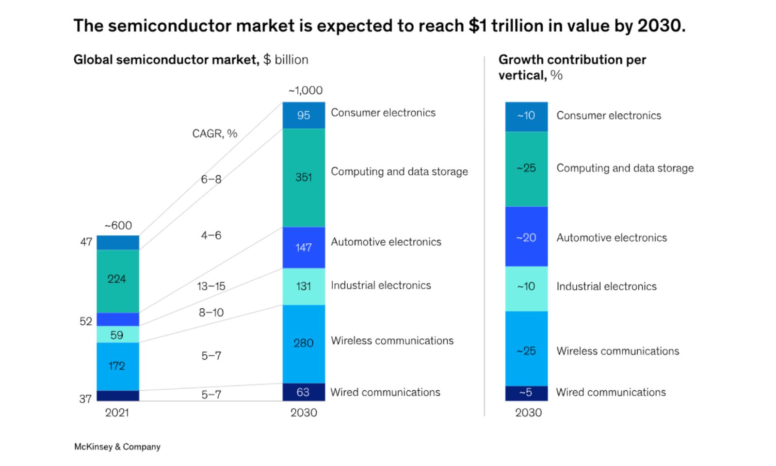
Projected semiconductor market growth by sector (2021–2030), with automotive, wireless communications, and data storage leading demand. Source: McKinsey & Company
The Hidden Pressures Behind Semiconductor Growth
Rapid growth in the semiconductor sector doesn't come cheap. The cost of building and outfitting a new fabrication plant is substantial, averaging close to $10 billion, and in some cases, even more2 . Meanwhile, the complexity of semiconductor equipment continues to grow, demanding ongoing R&D investments just to keep up with the demand3 .
The question remains: How to drive innovation, manage costs, and meet rising environmental expectations, all at once?
When the Margins Matter, So Do the Details
In a high-stakes industry like semiconductors, where equipment is fragile, high-value, and shipped globally, packaging plays a much bigger role than many realize. It affects nearly every cost driver in logistics:
- Freight class and shipping charges
- Storage and warehouse space
- Handling time and labor
- Transit damage and product loss
As supply chains become more regionalized and specialized, the packaging inefficiencies start to add up, both financially and environmentally.
That’s why Cost Take-Out (CTO) strategies are gaining momentum. They focus on redesigning packaging to:
- Reduce size and weight (cutting shipping and fuel costs)
- Simplify handling (saving time and labor)
- Lower the risk of in-transit damage
And crucially, the best solutions often support both bottom-line and sustainability goals.
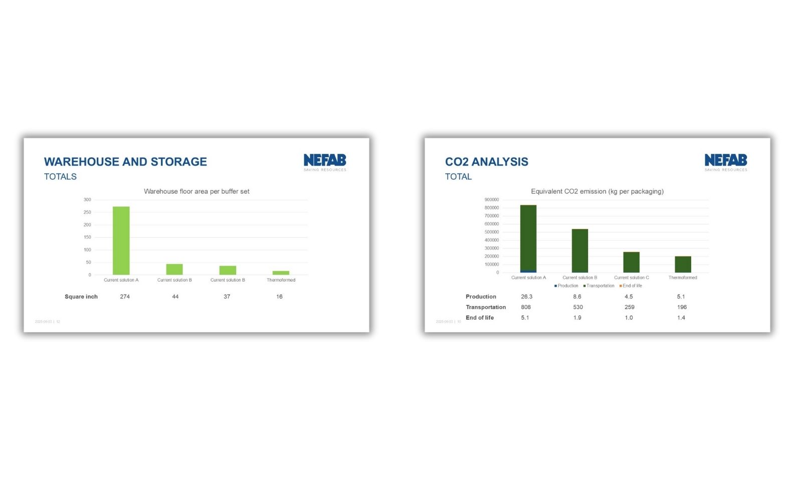
Packaging optimization delivered major reductions in emissions and logistics costs. Source: Nefab
Sustainability Is a Data-Driven Conversation
Environmental regulations are tightening. Customers and investors are asking tougher questions. As a result, sustainability performance is becoming a compliance and competitiveness issue. Yet packaging decisions are still, too often, made without understanding its impact, both on the environment and the bottom-line.
This is where Life Cycle Assessment (LCA) tools, like GreenCalc™, come in. They help companies:
- Quantify environmental impact by measuring CO₂-eq emissions, water and energy use, and material waste
- Model different logistics flows (e.g., one-way vs. returnable systems)
- Compare packaging options based on data, not assumptions
Incorporating CTO strategies and LCA tools allows businesses to turn packaging into a strategic asset, balancing regulatory compliance, environmental responsibility, and financial efficiency.
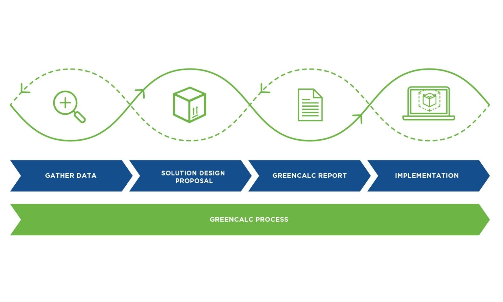
The four-step Life Cycle Assessment process helps evaluate packaging impact from design to implementation. Source: Nefab
Rethinking What Matters
As the semiconductor industry moves through a period of rapid change, the spotlight naturally lands on advances at the chip level. But resilience, cost efficiency, and sustainability aren’t just shaped by cutting-edge tech, they’re also influenced by the systems around it.
Packaging might not always get the attention, but when approached strategically, it can be a quiet driver of meaningful change.
As companies take a closer look at their supply chains for the decade ahead, it’s worth asking:
Where else could small shifts lead to big results?
We save resources in supply chains for a better tomorrow.
Want to learn more?
GET IN TOUCH
Contact us to learn more about our smart and sustainable solutions.
LEARN MORE
Solutions for the Semiconductor Industry
Sustainable Protection for Your Equipment
GreenCalc
Nefab’s own certified calculator measures and quantifies financial and environmental savings in our solutions
Global Supply & Local Services
With over 250 engineers across more than 38 locations, working together in a global network, you can count on us for your next packaging project.