Even the smallest vibrations or shock during transit can cause microscopic damage, leading to yield loss, qualification delays, or costly downtime at the fab. For quality assurance teams, the challenge often extends beyond fabrication, and it includes packaging, logistics, and post-shipping validation1.
That’s where engineered packaging solutions, like thermoformed Reflex cushioning, make a difference. Designed for consistency and precision, it preserves performance of delicate components through every handoff in the supply chain, ensuring zero-defect delivery and maintaining the integrity that production depends on.
The Impact of Transit Risk on Fab Performance
The journey of semiconductor manufacturing equipment and components from manufacturing site to fab is full of hidden threats, which can quietly undermine performance long before equipment is powered on:
- Vibrations and shocks can lead to micro-cracks or warping2
- Electrostatic Discharge (ESD) can damage sensitive electronics
- Particle contamination leads to additional cleaning before installation
- Temperature fluctuations might affect materials and coatings
Each of these risks can cause hidden but costly consequences. Packaging failures may not be visible at first glance, but their ripple effects are real. From missed delivery windows and production downtime to extended installation and requalification processes. When a component must be replaced or retested, urgent logistics and expedited shipping add another layer of expense and delay.

Every stage of semiconductor manufacturing equipment logistics must control vibration, ESD, and contamination to keep equipment fab-ready.
Why Foam Is No Longer a Perfect Fit for Fab-Grade Logistics
For decades, polyethylene (PE) foam has been the default cushioning for semiconductor components. But as the industry moves toward cleaner and more sustainable operations, foam’s limitations are hard to ignore. To start, PE often provides an inconsistent fit, allowing micro-movements that lead to vibration damage. It is also a single-use material that’s notoriously difficult to recycle, adding to waste and carbon emissions. Finally, it can shed particles, creating additional cleaning burdens inside fabs.3
The semiconductor sector’s commitment to precision and sustainability demands more advanced materials. Packaging, once an afterthought, must now match the same rigor as the processes it protects.
Thermoformed Reflex Cushioning: Protection Precision by Design
Thermoformed Reflex cushioning is reshaping how sensitive semiconductor manufacturing equipment moves through the supply chain.
Made from rigid, precisely molded recycled plastic, thermoformed inserts are tailored to the exact geometry of each component, ensuring a snug, stable fit during handling and long-distance transport. And the benefits are clear:
- Precision fit and consistency prevent micro-movement and vibration damage.
- Low outgassing and cleanroom compatibility protects sensitive components.
- Reusable and recyclable design supports circular logistics.
- Nefab’s lifecycle data shows significant emission reduction compared to PE foam.
Whether fully custom- for unique components or standardized for widely used semiconductor tools, thermoformed Reflex cushioning offers scalable, high-performance protection that aligns with the expectations of fab-grade operations.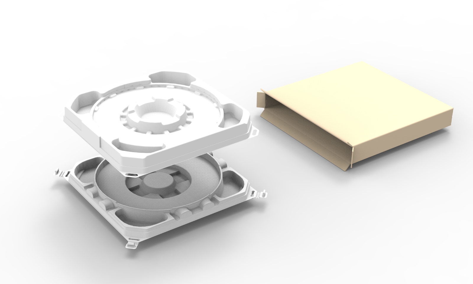
An engineered packaging solution featuring thermoformed cushioning precisely secures a high-purity ceramic semiconductor disc, ensuring its stability, cleanliness, and protection throughout global transit.
Standardization and Circular Logistics
Many semiconductor components are serviced or refurbished and reused. Their packaging should follow the same path. This not only supports corporate sustainability goals but also delivers tangible operational benefits:
- Lower total cost of ownership through reuse and reduced waste
- High cleanliness standards maintained through validated cleaning cycles
- Fewer packaging formats and simpler receiving operations
- Consistent performance across every shipping lane, handler and site
With global OEMs aiming to harmonize packaging across facilities and suppliers, thermoformed cushioning enables them to validate once and deploy everywhere, a key advantage for global supply chain efficiency.
Engineering Confidence into Every Shipment
Packaging is more than a protective layer, it’s a critical link in delivering semiconductor equipment that performs exactly as designed. By investing in engineered protection, OEMs and suppliers translate packaging precision directly into:
- Higher uptime
- Faster installation and qualification
- Reduced waste and emissions
- Consistent, fab-ready delivery
In an industry defined by precision, packaging deserves the same level of engineering excellence, because in semiconductor logistics, perfection doesn’t stop at the fab door.
We save resources in supply chains for a better tomorrow.
Want to learn more?
GET IN TOUCH
Contact us to learn more about our smart and sustainable solutions.
LEARN MORE
Solutions for the Semiconductor Industry
Sustainable Protection for Your Equipment
GreenCalc
Nefab’s own certified calculator measures and quantifies financial and environmental savings in our solutions
Global Supply & Local Services
With over 250 engineers across more than 38 locations, working together in a global network, you can count on us for your next packaging project.