Packaging solutions that protect your semiconductor equipment and components
Custom sustainable packaging solutions keeping them safe, clean, and secure throughout their entire logistical journey

Custom sustainable packaging solutions keeping them safe, clean, and secure throughout their entire logistical journey
Transporting high-value, sensitive semiconductor equipment isn’t only about moving products—it’s about meeting strict cleanroom standards, maintaining absolute quality, and ensuring every component arrives flawless and ready for action.
At Nefab, we don’t just provide packaging—we deliver solutions. Our custom packaging is designed and manufactured using a range of materials carefully selected by our global team of engineers. Nefab’s solutions focus on minimizing material use without compromising safety, delivering sustainable, protective, and tailored packaging for every shipment.
With 6 ISTA-certified test labs worldwide, including in key semiconductor regions, Nefab ensures the safe transportation of your products at every stage of the supply chain.
At Nefab, we specialize in designing, manufacturing, and cleaning cleanroom-compliant packaging solutions, ensuring your products are ready for transport.
We deliver measurable change by leveraging data through our GreenCalc™ Life Cycle Analysis (LCA) tool, providing insights that drive both financial and environmental savings.

Nefab collaborated with a semiconductor manufacturer to optimize their wafer packaging solution, delivering substantial financial and environmental benefits.
Nefab partnered with a leading semiconductor manufacturer to optimize the packaging solution for shipping wafers between its front-end and back-end facilities, achieving significant financial and environmental benefits.

Our customer was using a legacy packaging design for the RPS (Remote Plasma Source) Adapters that was inefficient and costly. By re-engineering the packaging, we developed a streamlined, resource-efficient solution that reduced material use and volumetric weight.
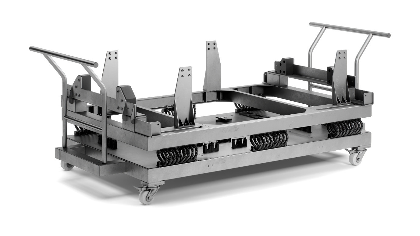
A leading innovator in the semiconductor industry required a specialized packaging solution for hoisting tools used in their cleanrooms. Through a multi-layered, material-specific design they improved cleanliness, efficiency, and product security.

A customer in the semicon sector faced high air freight costs, product safety concerns, and inefficient handling processes. By implementing the ExPak XL system, the customer achieved a 40% reduction in packaging weight, significantly lowering transportation costs and CO2 emissions.
When we say we offer complete packaging solutions, we really mean it. Our packaging and added-value services support you at every stage of the logistical process.
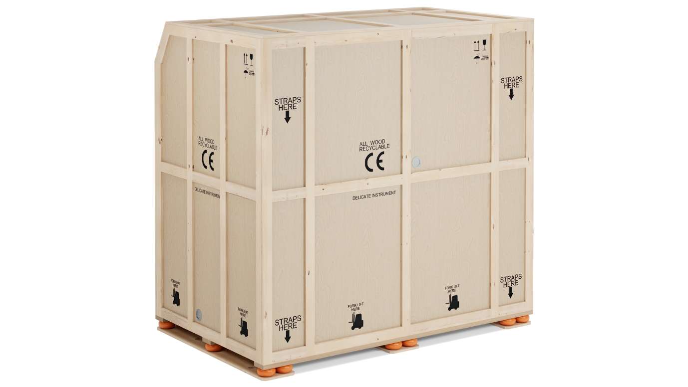
Whether you're shipping semiconductor manufacturing equipment one-way or in returnable flow, we’ve got you covered with a wide range of innovative crating solutions.
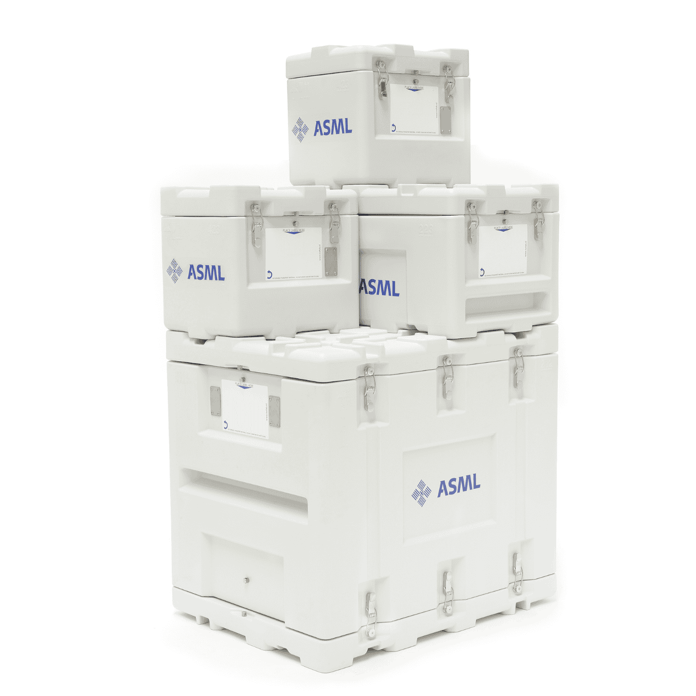
Our lightweight, highly customizable plastic-based solutions are easy-to-clean which makes them ideal for packaging a range of products, from server media packs to ceramics and quartz items.
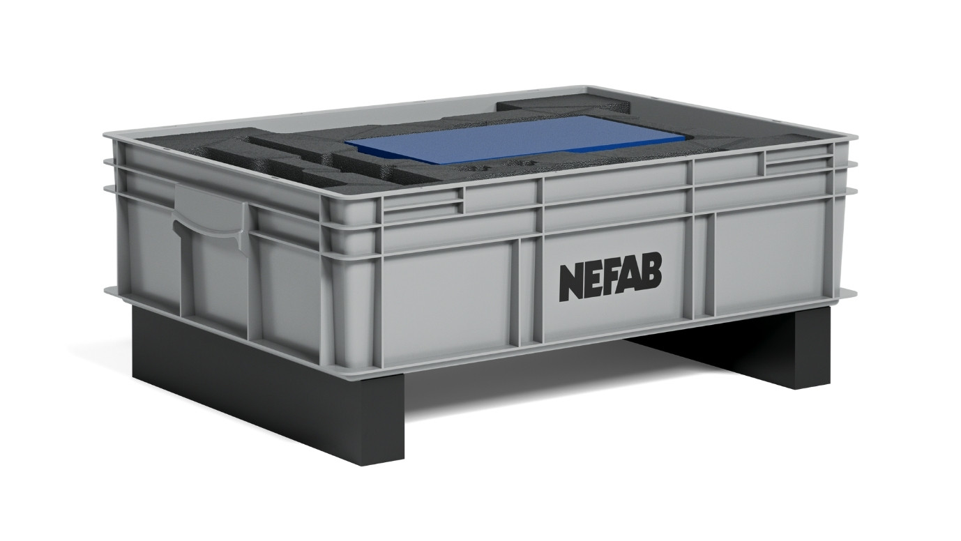
Nefab offers engineered packaging solutions tailored to customer requirements, meeting ISO 5 and ISO 7 cleanroom standards. Our solutions are dedicated for returnable and expendable flows such as KLT boxes with customized interiors, PP boxes, plastic pallets, steel assemblies, flight cases, cleanroom bags.
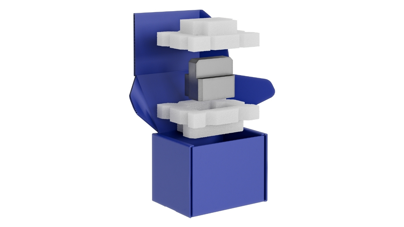
Our packaging solutions are designed to minimize material use while ensuring optimal product protection, perfect for sensitive environments. We offer a range of expendable complete packaging solutions, including PE foams, PP boxes, thermoformed trays, bags, foils, desiccants, membrane boxes, and tapes.
Whether standard or customized, each product is tailored for supply chain efficiency in transportation, allowing safe handling and storage of critical components.
We offer several types of logistics and value added services to streamline operations for customers within the semiconductor industry

We provide comprehensive cleanroom services for products and tools such as: cleaning services according to ISO class 5 and 7 at Nefab cleanroom or at the customer`s cleanrooms if prepared. Assembly and kitting services. Custom bag production. Custom cleanroom packaging design and development.
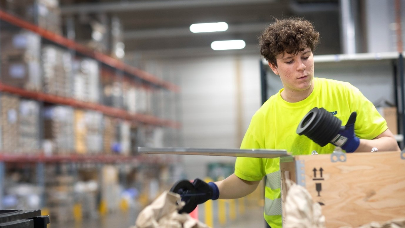
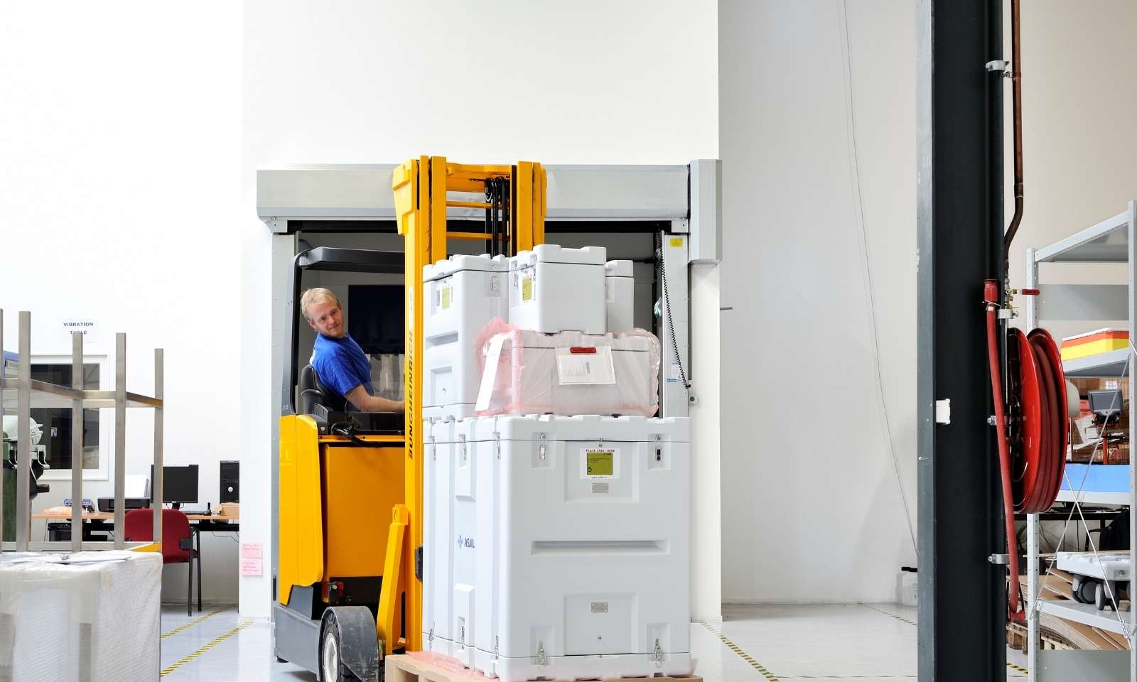
Nefab offers on-site packing services tailored to your needs, ensuring safe, secure packing and loading, whether in your cleanroom, warehouse, or at our facility.

Nefab’s digital services simplify tracking of returnable packaging, ensure security with high-value asset management, and optimize installation planning and monitoring for smoother operations.
Our digital solutions help eliminate blind spots in supply chains. With track-and-trace capabilities all shipments can be monitored with full control and visibility. This lets you track the location and condition of your assets while managing their flow. Our platforms work on any device or network and can be customized for your products and supply chains

Nefab is more than just a packaging provider - we also offer:
We combine global reach with local knowledge to provide tailored solutions wherever you are.
Our strict quality control processes, supported by our ISO-certified Quality Management System, ensure the safety and reliability of your products, wherever they go.
At Nefab, it’s not just about what we do—it’s how we make it better, together.

Ewa Rosinek
Global Segment Director Semiconductors
Join us in transforming the future of semiconductor packaging. Contact us today to find out how our bespoke solutions can add value to your logistic needs and contribute to a sustainable footprint within the industry.
Write your future in clean, sustainable, and efficient packaging -- With Nefab, you're covered on all fronts.
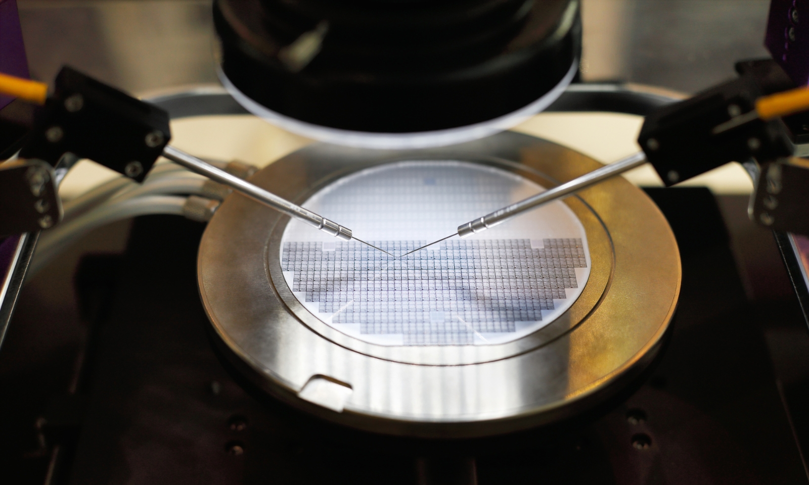
Semiconductor manufacturing leaves no room for error. Every process, every component, every piece of equipment operates within microscopic tolerances, and that precision can’t be compromised once the machines leave the cleanroom.

As geopolitical tensions, demand for advanced chips, and national self-sufficiency strategies reshape global production, manufacturers are investing heavily in regionalized, resilient supply chains.

Tackling the challenge of decarbonizing the semiconductor industry is no small feat. A crucial first step is for companies to accurately assess their current greenhouse gas (GHG) emissions.