隨著地緣政治緊張局勢、對先進晶片的強勁需求以及各國自給自足戰略重塑全球生產格局,製造商正大力投資於區域化且具韌性的供應鏈。
到2030年,該產業預計將投資逾1兆美元於新建半導體晶圓廠1 儘管成長前景廣闊,製造商同時面臨嚴峻挑戰,使得成本效益與永續性較以往任何時候都更為關鍵。
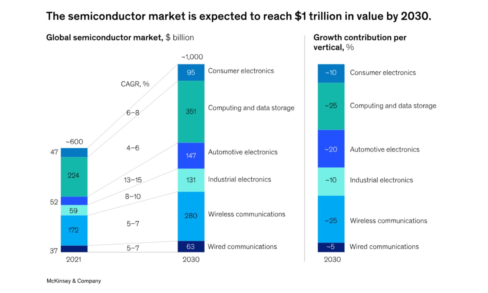
各領域半導體市場預測增長(2021–2030),其中汽車、無線通訊及數據儲存領域需求領先。資料來源:麥肯錫公司
半導體增長背後的隱性壓力
半導體產業的快速成長代價不菲。新建一座晶圓廠的建設與設備成本相當龐大,平均接近100億美元,某些情況下甚至更高。2 。與此同時,半導體設備的複雜度持續攀升,僅是為了滿足需求,就必須持續投入研發資金3 。
問題依然存在:如何同時推動創新、管控成本,並滿足日益提升的環保期望?
當邊際效益至關重要時,細節同樣不容忽視
在半導體這類高風險產業中,設備既脆弱又價值高昂,且需全球運輸,包裝所扮演的角色遠比多數人認知的更為關鍵。它幾乎影響物流中的所有成本驅動因素:
- 貨運等級與運費
- 倉儲空間
- 處理時間與人力
- 運輸損壞與產品損失
隨著供應鏈日益區域化與專業化,包裝效率低下的問題開始在財務與環境層面累積成問題。
正因如此,成本削減策略(CTO)正日益受到重視。這些策略著重於重新設計包裝,以達成以下目標:
- 減輕尺寸與重量(降低運輸與燃料成本)
- 簡化處理流程(節省時間與人力)
- 降低運輸過程中的損壞風險
關鍵在於,最佳解決方案往往同時支持盈利目標與永續發展目標。
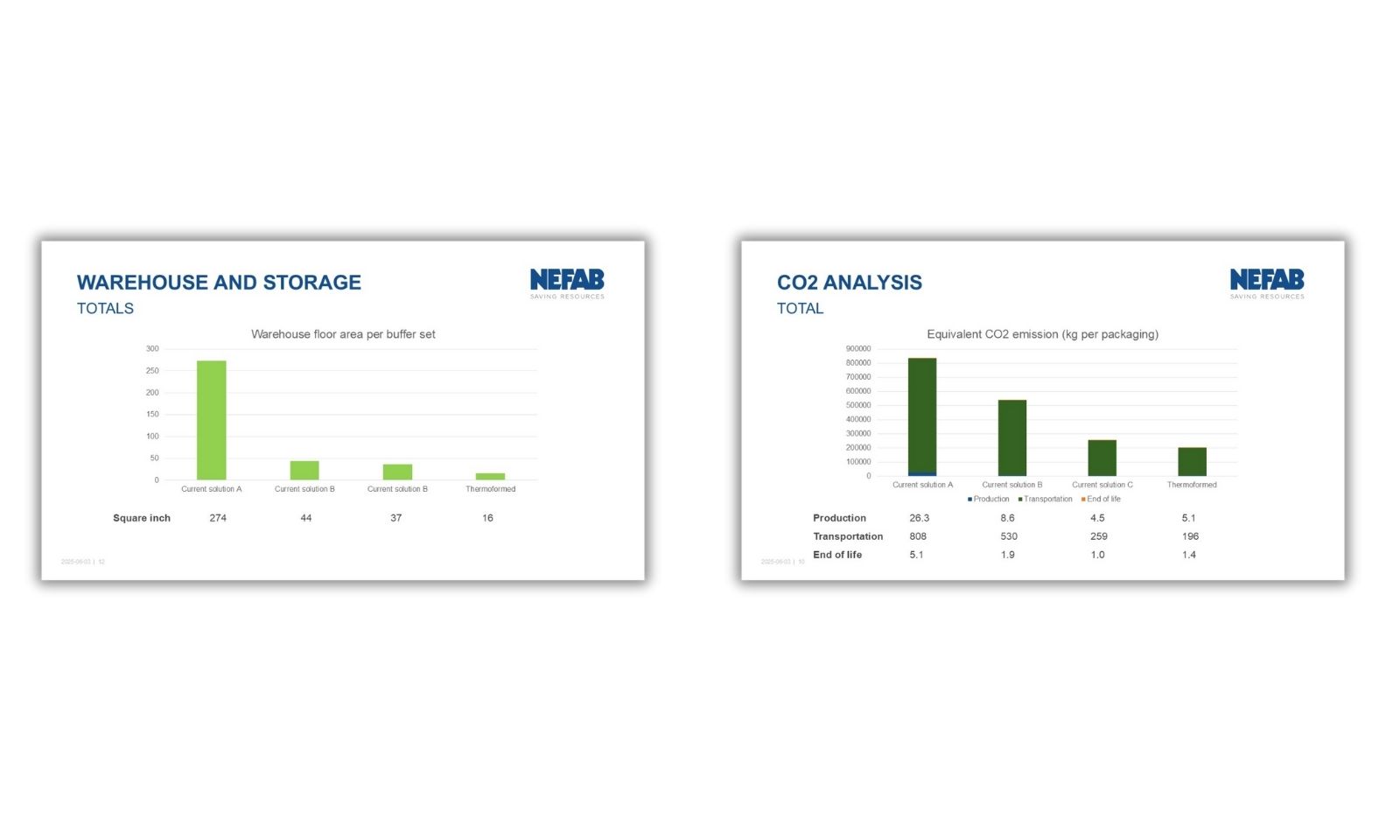
包裝優化大幅降低了排放量與物流成本。來源:Nefab
永續發展是一場數據驅動的對話
環保法規日益嚴格。客戶與投資者提出更嚴苛的質疑。因此,永續發展績效正逐漸成為合規與競爭力的關鍵議題。然而,包裝決策仍經常在未充分理解其對環境與企業獲利雙重影響的情況下草率作出。
這正是生命週期評估(LCA)工具(如GreenCalc™)發揮作用之處。它們協助企業:
- 透過量測二氧化碳當量排放量、水資源與能源消耗量及物料廢棄物,量化環境影響
- 建模不同的物流流程(例如:單向系統與可回收系統)
- 根據數據而非假設來比較包裝方案
整合技術長策略與生命週期評估工具,能讓企業將包裝轉化為戰略資產,在法規遵循、環境責任與財務效益之間取得平衡。
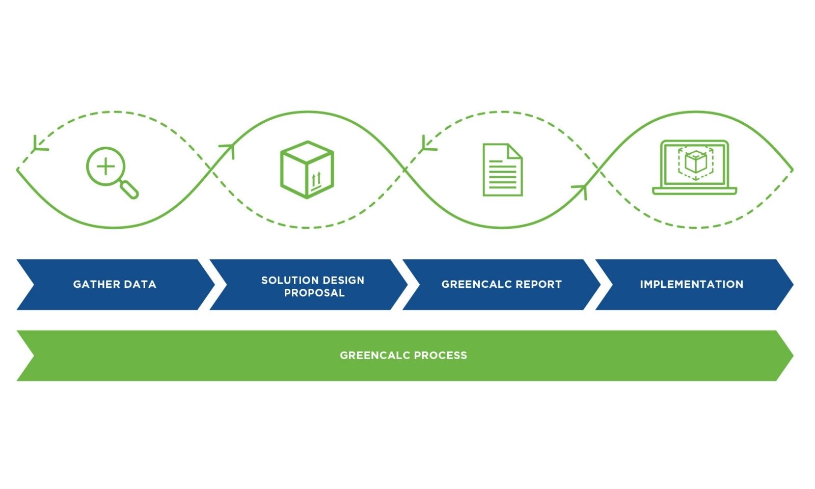
四階段生命週期評估流程有助於評估包裝從設計到實施的整體影響。來源:Nefab
重新思考什麼才是重要的
隨著半導體產業經歷快速變革的時期,焦點自然落在晶片層面的技術突破。然而,韌性、成本效益與永續性不僅取決於尖端技術,更受其周邊系統的形塑影響。
包裝或許不總能獲得關注,但若以策略性方式處理,它便能成為推動深遠變革的靜默推手。
隨著企業開始審視未來十年的供應鏈佈局,值得思考的是:
還有哪些領域能透過微調帶來顯著成效?
為了更美好的明天,我們在供應鏈中節約資源。
想瞭解更多資訊?
聯繫我們
聯繫我們 ,詳細瞭解我們的智慧和可持續解決方案。
瞭解更多資訊
半導體產業解決方案
為您的設備提供永續保護
GreenCalc
Nefab 自己的認證計算器測量和量化我們解決方案中的財務和環境節約情況
全球供應與在地服務
我們擁有超過250名工程師,遍佈38個以上據點,透過全球網絡協同合作,您可放心將下一個包裝專案交給我們。