挑戰:在亞洲市場開發具成本效益的光纖解決方案
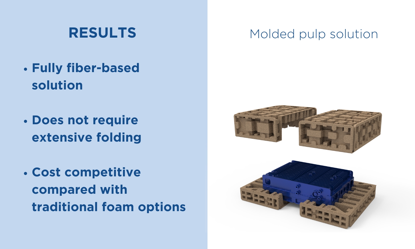
在亞洲地區取代塑膠材料面臨困難,主因在於聚乙烯泡棉的成本競爭力。雖然纖維解決方案在歐美地區成效顯著,但對亞洲客戶而言成本過高。為避免阻礙客戶的轉型進程,我們決定引進模塑紙漿作為替代方案。
Nefab的解決方案:透過協作創新,打造永續且實用的替代方案
Nefab提出了一種模塑紙漿解決方案。經過多次設計迭代與客戶進行廣泛的聯合測試後,我們最終達成了一項設計方案,該方案在測試中未被提出任何異議,完全符合測試標準。
在電信領域,包裝材料正廣泛轉向纖維基材。為加速客戶的纖維化轉型,我們持續探索新方向。某主要客戶目標在2030年前實現包裝材料近100%採用纖維材質。數年前啟動的轉型進程中,我們攜手逐步以纖維替代方案取代塑膠解決方案。
在亞洲地區取代塑膠材料面臨困難,主因在於聚乙烯泡棉的成本競爭力。雖然纖維解決方案在歐美地區成效顯著,但對亞洲客戶而言成本過高。為避免阻礙客戶的轉型進程,我們決定引進模塑紙漿作為替代方案。
Nefab提出了一種模塑紙漿解決方案。經過多次設計迭代與客戶進行廣泛的聯合測試後,我們最終達成了一項設計方案,該方案在測試中未被提出任何異議,完全符合測試標準。
憑藉此成功經驗,我們期望與客戶攜手合作,將此解決方案推廣至更多市場。同時,我們也將評估其他適用於此類包裝的產品,以協助客戶順利轉型至纖維材質。
最終設計將永續性與客戶重視的塑膠解決方案功能性相結合。關鍵成果包括:
我們的模塑紙漿解決方案提供全纖維基底、具成本競爭力的塑膠泡棉替代品,即使在價格最敏感的市場中,也能協助您達成永續發展目標。我們與您攜手合作,共同設計、測試並實施有效的包裝方案。
與我們的專家洽談
深入探索我們為電信產業打造的智慧永續解決方案,了解我們如何協助客戶達成財務與環保目標。
探索電信解決方案頁面
發掘專為電信產業設計的全面性包裝與物流解決方案。
Nefab在瓜達拉哈拉擴建了業務,新建一座佔地3,000平方公尺的生產與工程設施,強化對墨西哥西部先進製造及數位基礎建設產業的支援。
《商業焦點》雜誌最新一期刊載了一篇深度專題報導,您可透過此文進一步了解Nefab對創新的持續深化承諾,尤其在環保型可循環解決方案領域的耕耘。
隨著產量增加及自動化在電池工廠日益普及,包裝功能不再僅限於保護零件在運輸過程中的安全。焦點轉向能保持形狀、在重複使用循環中更持久耐用,並在每次運輸中持續穩定運作的解決方案。