挑戰:
安裝現場面臨交付不一致且分散的問題:無線電設備由製造商直接送達,而配件與安裝材料則由多家第三方供應商分別運送。這導致頻繁出現延遲或部分到貨的情況,組件不匹配,以及現場耗時的套件組裝與倉儲作業。缺乏標準化包裝降低了現場套件的可視性與管控能力,增加了人力與處理成本,並限制了貨櫃利用率,最終導致運輸成本上升、交貨週期延長,以及延誤與返工風險增加。
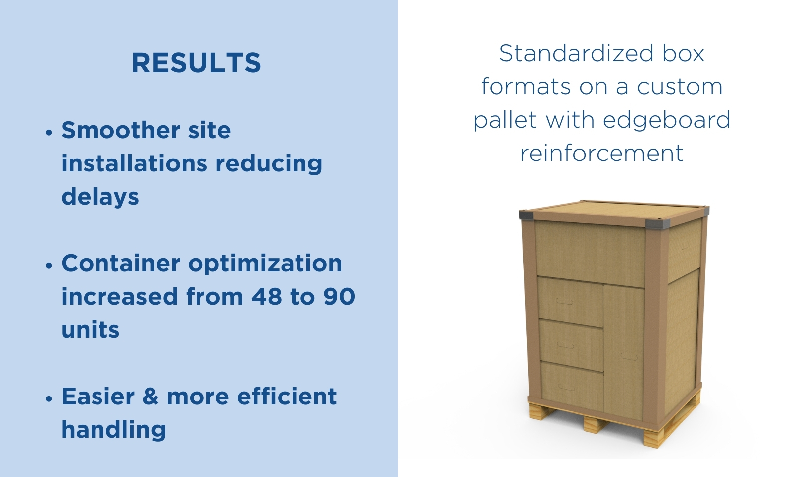
Nefab 的解決方案:
Nefab實施了一項包裝解決方案,將製造商與多家第三方供應商的物料整合至單一可堆疊瓦楞紙套件中——採用「單一工地,單一箱體」的策略。 此設計採用兩種標準化箱型,置於加裝邊板強化結構的客製化托盤上,既能保護組件又能實現安全堆疊以利貨櫃運輸。此方案使現場安裝所需的所有物品得以整合包裝、單一單位運輸,並在現場直接拆箱使用,無需額外組裝。此舉不僅提升物料可視性與防護性、優化貨櫃利用率,更有效減少搬運作業、運輸損壞及單位運費成本。