- News & Insights
- 2025
- Sustainable Packaging for Wafer Shipping
- Customer Cases
- Semiconductor
Sustainable Packaging for Wafer Shipping
Semiconductor manufacturing is a complex process that can be broadly divided into two main phases: the front-end process and the back-end process. Nefab partnered with a leading semiconductor manufacturer to optimize the packaging solution for shipping wafers between its front-end and back-end facilities, achieving significant financial and environmental benefits.
The Challenge: Optimizing Packaging for Cost Efficiency and Sustainability in Air Freight
The customer, a multinational manufacturer of integrated circuits, relied on a packaging solution consisting of an inner and outer box with PU foam corners to ship wafers by air. For bulk shipments, a multi-pack pallet was used, which was often only partially filled. Since air freight costs are charged based on volumetric weight, this resulted in excessive transportation expenses and inefficient use of space. In addition, the use of PU foam raised environmental concerns.
Nefab’s Solution for Wafer Shipping
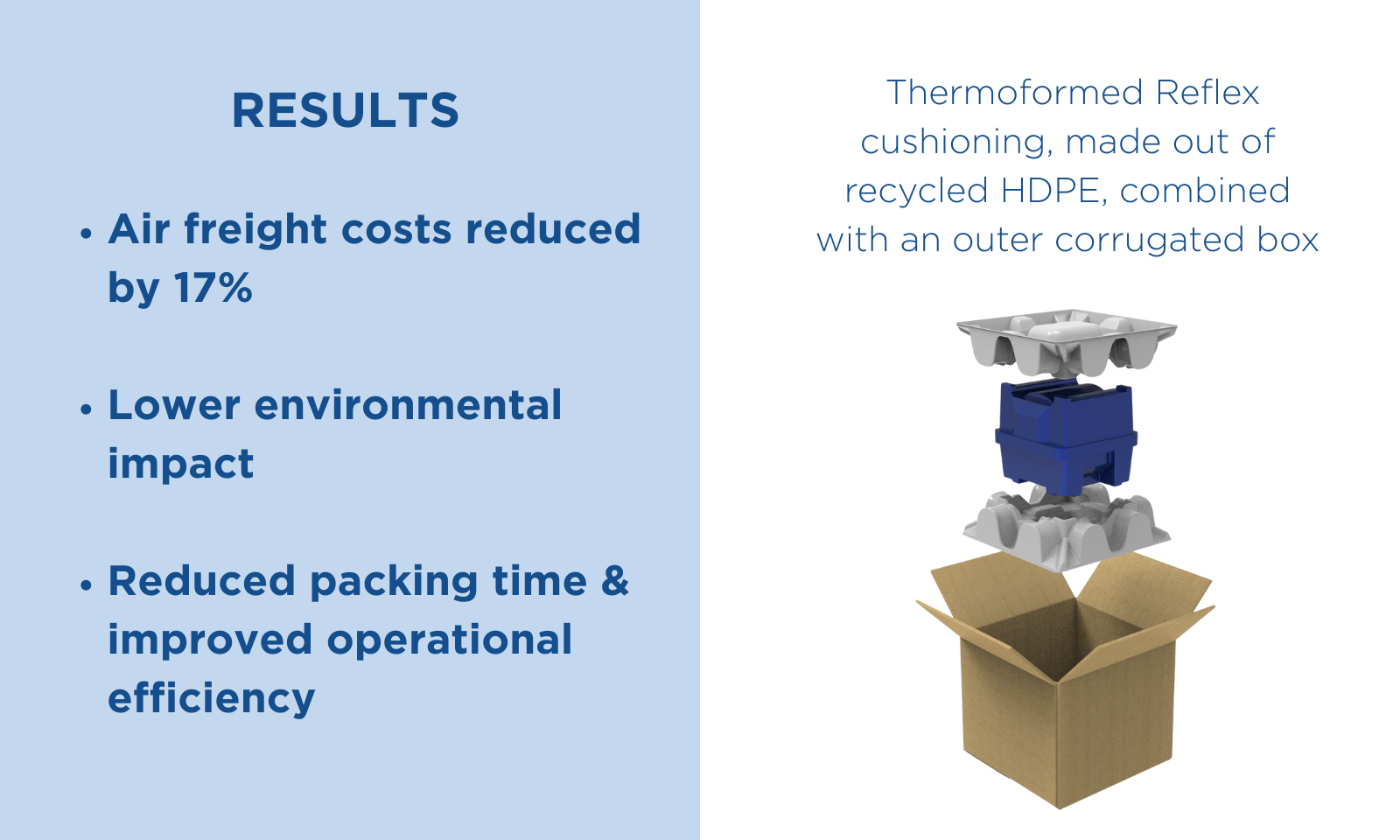
To address these challenges, Nefab developed a redesigned packaging solution featuring thermoformed Reflex cushioning, made out of recycled HDPE, combined with an outer corrugated box. The solution delivered the following improvements:
- Reduced volumetric weight: A 17% reduction in volumetric weight compared to the previous solution.
- Environmentally friendly design: Replacement of PU foam from virgin plastics with recycled HDPE trays.
- Optimized assembly process & standardization: Simplified packing steps, which were implemented across multiple facilities.
"By replacing PU foam with recycled HDPE and reducing volumetric weight by 17%, Nefab’s innovative packaging solution streamlined operations across multiple facilities."
The Results: Driving Cost Savings, Sustainability, and Efficiency
The implementation of Nefab’s solution delivered measurable benefits across cost, sustainability, and process efficiency:
- Cost savings: Air freight costs were reduced by 17%, resulting in annual savings of approximately $160,000.
- Lower environmental impact: CO₂ emissions decreased by 9%, equivalent to 48 metric tons, thanks to reduced volumetric weight and the use of recycled materials.
- Streamlined packing process & improved consistency: This solution resulted in a reduction of packing time and improved operational efficiency.
By introducing this innovative packaging solution, Nefab helped the customer achieve both financial and environmental savings while optimizing logistics operations.
We save resources in supply chains for a better tomorrow.
Explore our Semicon Industry Solutions
See our comprehensive packaging and logistics services designed specifically for the medical sector.
Explore Semicon Industry Solutions
See our comprehensive packaging and logistics services designed specifically for the medical sector.
Explore More Insights
Additional Resources